Multichannel silicon substrate wavelength division multiplexing high-speed optical transmitting-receiving integral device

A wavelength division multiplexing, optical transceiver technology, applied in optical components, instruments, optics, etc., can solve problems such as low integration, large device size, and unfavorable miniaturization.

Inactive Publication Date: 2017-09-12
HUAZHONG UNIV OF SCI & TECH
View PDF4 Cites 20 Cited by
  • Summary
  • Abstract
  • Description
  • Claims
  • Application Information

AI Technical Summary

Problems solved by technology

[0003] The typical schemes that already exist in the prior art include: 1. The free optical space scheme based on wavelength division multiplexing filters. This scheme has as many as dozens of optical passive devices, and the assembly process is very complicated, the cost is high, and the size is small. Large, low integration, difficult to meet higher speed devices; Second, based on silicon dioxide planar optical waveguide technology transceiver devices, this scheme separates the transceiver devices, and the transceiver devices each require a ceramic airtight case, ceramic Airtight housings are usually expensive, so this solution has the

Method used


Image

  • Multichannel silicon substrate wavelength division multiplexing high-speed optical transmitting-receiving integral device
  • Multichannel silicon substrate wavelength division multiplexing high-speed optical transmitting-receiving integral device
  • Multichannel silicon substrate wavelength division multiplexing high-speed optical transmitting-receiving integral device

Examples


Embodiment Construction

[0027] In order to make the object, technical solution and advantages of the present invention clearer, the present invention will be further described in detail below in conjunction with the accompanying drawings and embodiments. It should be understood that the specific embodiments described here are only used to explain the present invention, not to limit the present invention. In addition, the technical features involved in the various embodiments of the present invention described below can be combined with each other as long as they do not constitute a conflict with each other.

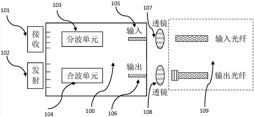
[0028] The multi-channel silicon-based wavelength division multiplexing high-speed optical transceiver integrated device proposed by the present invention includes a transmitting unit and a receiving unit, the output end of the planar optical waveguide chip is connected to the output optical fiber, and the input end of the planar optical waveguide chip is connected to the input optical fiber: Th...


PUM


Abstract

The invention discloses a multichannel silicon substrate wavelength division multiplexing high-speed optical transmitting-receiving integral device which comprises a transmitting unit and a receiving unit, wherein the transmitting unit and the receiving unit are coupled with a planar optical waveguide chip; a wave division unit and a wave combining unit are arranged on the planar optical waveguide chip; the input end and the output end of the planar optical waveguide chip are respectively coupled with an input optical fiber and an output optical fiber correspondingly. On the basis of a silicon photon technique, a multichannel high-speed transmitting unit and a multichannel high-speed receiving unit are integrated, multiple transmission velocities can be compatible, the integration degree is increased, the sealing process is simplified, the cost is effectively lowered, and very high practical values are made.

Description

technical field [0001] The invention belongs to the field of integrated optical structures in the field of optical fiber communication, and in particular relates to a multi-channel silicon-based wavelength division multiplexing high-speed optical transceiver integrated device. Background technique [0002] In recent years, with the popularization of smart devices (computers, mobile phones, smart wearable devices), the amount of data in optical fiber communication networks has shown explosive growth. 40Gb / s optical modules have been deployed on a large scale, and 100Gb / s optical modules have also been gradually mass-produced. Deployment, 200Gb / s optical devices are also in the research and development stage. In order to meet market demand, it is imperative to develop high-speed optical communication devices in the direction of small size, high integration, low power consumption, and low cost. In dense wavelength division or frequency division multiplexing systems, it is nece...

Claims


Application Information

Patent Timeline
IPC IPC(8): G02B6/42
CPCG02B6/4246G02B6/4204G02B6/4214
Inventor 夏金松刘俊陶诗琦朱良秋黄庆忠
Owner HUAZHONG UNIV OF SCI & TECH
Why Eureka
Try Eureka