
Array substrate, display panel, and testing method of display panel

A technology of array substrate and testing method, which is applied in the direction of housing with display/control unit, electronic circuit testing, printed circuit testing, etc., to achieve the effects of saving space, reducing power consumption, and solving insufficient driving capabilities

Inactive Publication Date: 2017-09-12
XIAMEN TIANMA MICRO ELECTRONICS
View PDF9 Cites 22 Cited by
  • Summary
  • Abstract
  • Description
  • Claims
  • Application Information

AI Technical Summary

Problems solved by technology

[0005] The present invention provides an array substrate, a display panel and a testing method for the display panel to solve the problems in the existing VT testing process and realize the design of the lower narrow frame of the display panel

Method used


Image

  • Array substrate, display panel, and testing method of display panel
  • Array substrate, display panel, and testing method of display panel
  • Array substrate, display panel, and testing method of display panel

Examples


Embodiment Construction

[0038] The present invention will be further described in detail below in conjunction with the accompanying drawings and embodiments. It should be understood that the specific embodiments described here are only used to explain the present invention, but not to limit the present invention. In addition, it should be noted that, for the convenience of description, only some structures related to the present invention are shown in the drawings but not all structures.

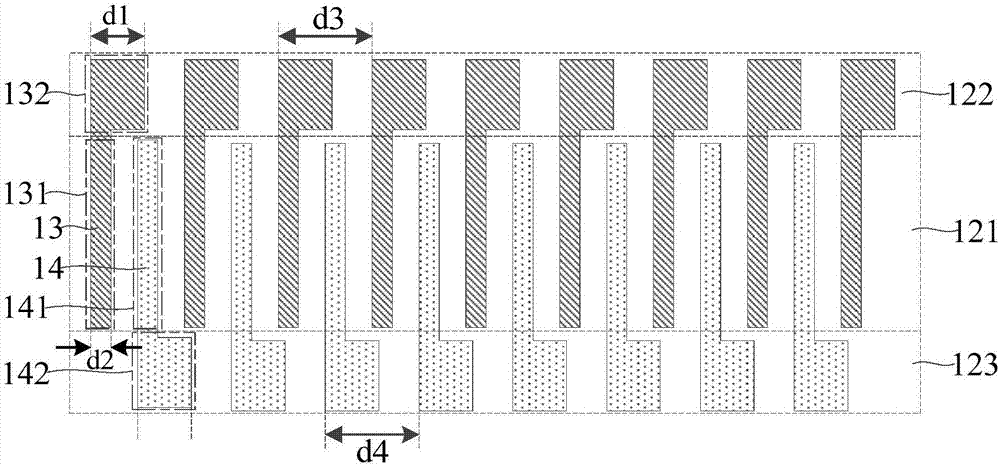
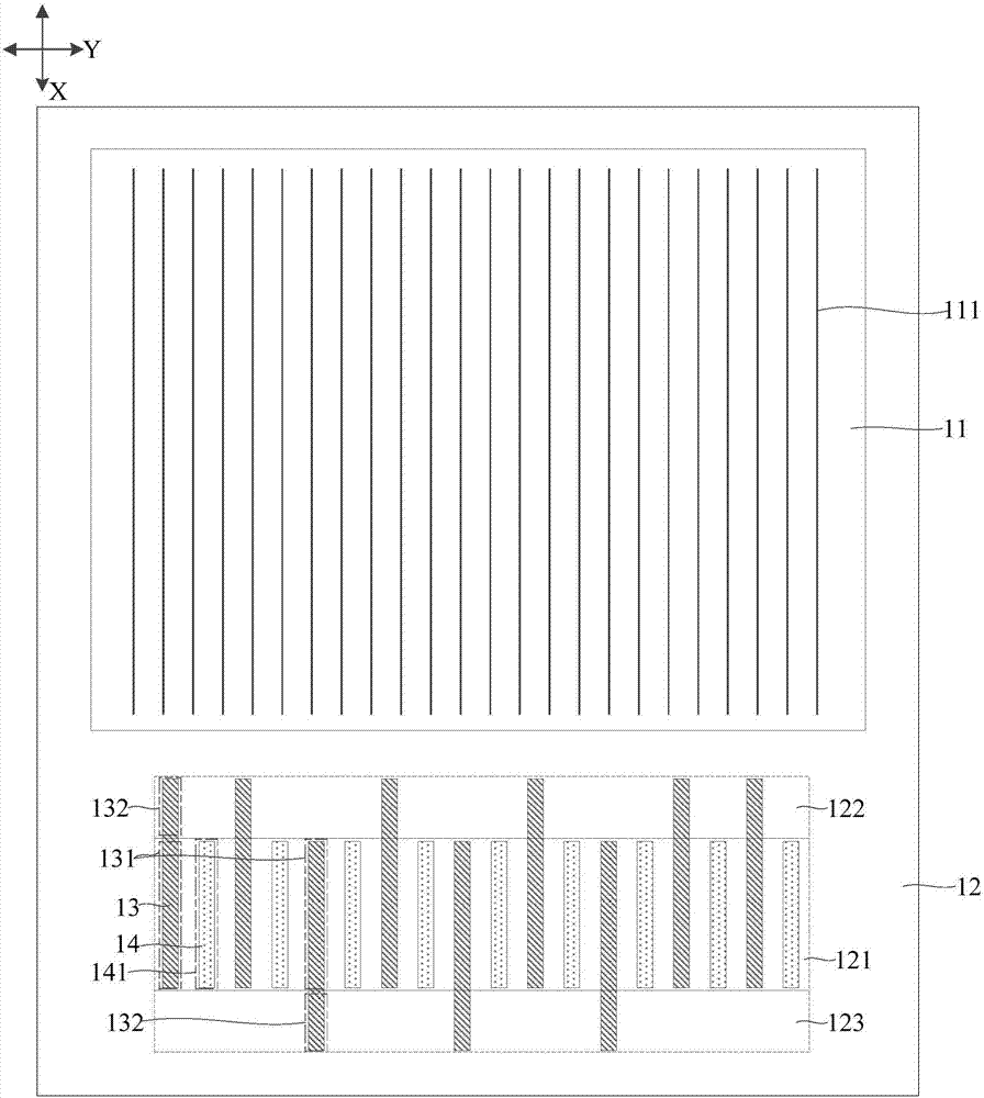
[0039] Figure 2A It is a schematic structural diagram of an array substrate provided by an embodiment of the present invention. see Figure 2A , the array substrate, comprising:

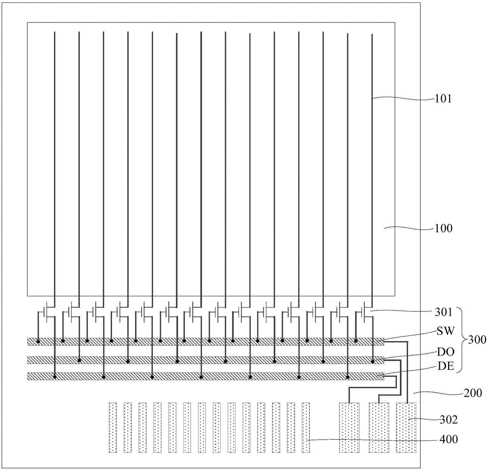
[0040] A plurality of display signal lines 111 located in the display area 11;

[0041] A plurality of first bonding pads 13 and a plurality of second bonding pads 14 are located in the peripheral region 12 surrounding the display region 11 , and are respectively connected to a plurality of display signal lines 111 correspondingly. ...


PUM


Abstract

The invention discloses an array substrate, a display panel, and the testing method of the display panel. The array substrate comprises a plurality of display signal lines, which are disposed on the display area; a plurality of first bonding pads and a plurality of second bonding pads, which are disposed on a peripheral area around the display area, and are correspondingly connected with the plurality of display signal lines; a first testing area and a second testing area, which are disposed on two sides of a main body area along a first direction. The first bonding pads comprise first main body parts, and the second bonding pads comprise second main body parts. The first main body parts and the second main body parts are disposed on the main body area, and are arranged at intervals along a second direction. At least a part of the first bonding pads comprise first testing parts, and at least a part of the second bonding pads comprise second testing parts. The first testing parts are disposed on the first testing area, and the second testing parts are disposed on the second testing area. By adopting the technical scheme provided by the invention, a VT detection circuit is saved, and the lower narrow edge frame space of the display panel is saved.

Description

technical field [0001] Embodiments of the present invention relate to the field of display technology, and in particular, to an array substrate, a display panel, and a testing method for the display panel. Background technique [0002] Before the display panel leaves the factory, it is necessary to perform visual inspection (VT inspection) on the display panel to detect whether the display panel can work normally. [0003] figure 1 It is a structural schematic diagram of a display panel in the prior art. see figure 1 , the display panel includes a display area 100, the display area 100 is provided with a plurality of data signal lines 101, and the non-display area 200 is provided with a plurality of display pads 400, and the display pads 400 are correspondingly connected to the plurality of data signal lines 101 (specifically connection not shown). The display panel also includes a VT detection circuit 300, and the VT detection circuit 300 includes a plurality of thin fi...

Claims


Application Information

Patent Timeline
Patent Type & Authority Applications(China)
IPC IPC(8): G09G3/00
CPCG09G3/006H05K1/0268H05K3/361H05K2201/09709H05K2201/10128G02F1/13458G02F1/1362G09G2300/0426H01L27/1244G02F1/136254H05K5/0017G01R31/282H05K1/0296G01R31/2808H05K1/111H01L27/1214
Inventor 周洪波
Owner XIAMEN TIANMA MICRO ELECTRONICS
Learn More