Array substrate, touch display module, electronic equipment and fingerprint identification method

An array substrate and touch display technology, which is applied in the electronic field, can solve the problems of limited fingerprint chip size, low touch precision, and large thickness, and achieve the effects of improving touch sensing ability, reducing design difficulty, and facilitating use

Inactive Publication Date: 2017-09-15
SHANGHAI YUDE TECH CO LTD
View PDF8 Cites 4 Cited by
  • Summary
  • Abstract
  • Description
  • Claims
  • Application Information

AI Technical Summary

Problems solved by technology

[0003] The inventors of the present invention found in the process of realizing the present invention that: since the current fingerprint identification modules in mobile phones are mostly based on the principle of capacitance, and by packaging the fingerprint sensing chip made by the wafer process in an LGA (Land Grid Array) ) Packaging technology After being packaged into a module, it is then integrated into mobile phone products. Therefore, limited by the size of the fingerprint chip, the area where the fingerprint recognition function can be realized is currently very small, and it is very inconvenient for users to use.
Moreover, the fingerprint identification module needs to be packaged separately and then assembled into electronic equipment, which is a cumbersome process.
However, most touch solutions use independent capacitive screen modules, which have low touch accuracy and large thickness.

Method used


Image

  • Array substrate, touch display module, electronic equipment and fingerprint identification method
  • Array substrate, touch display module, electronic equipment and fingerprint identification method
  • Array substrate, touch display module, electronic equipment and fingerprint identification method

Examples


Embodiment Construction

[0029] In order to make the object, technical solution and advantages of the present invention clearer, various embodiments of the present invention will be described in detail below in conjunction with the accompanying drawings. However, those of ordinary skill in the art can understand that, in each implementation manner of the present invention, many technical details are provided for readers to better understand the present application. However, even without these technical details and various changes and modifications based on the following implementation modes, the technical solution claimed in this application can also be realized.

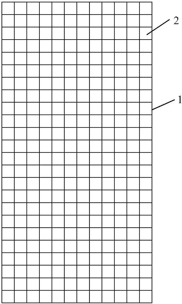
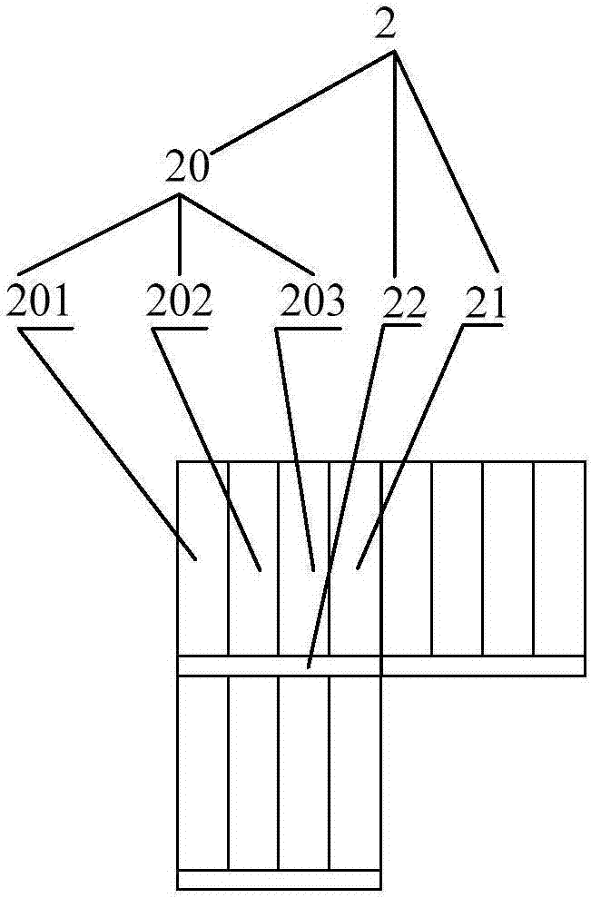
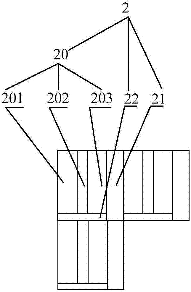
[0030] The first embodiment of the present invention relates to an array substrate, which is applied in a touch display module. Wherein, the display module of the touch display module can be AMOLED (Active Matrix / Organic Light Emitting Diode, active matrix organic light emitting diode), LCD (Liquid Crystal Display, liquid crystal display), ...


PUM


Abstract

The invention relates to the technical field of electronics, and discloses an array substrate, a touch display module, electronic equipment and a fingerprint identification method. The array substrate comprises a substrate body and first basic points arranged on the substrate body like a matrix, wherein the first basic points comprise a display pixel, a fingerprint pixel and a touch pixel arranged together; and the substrate body comprises signal lines of the display pixel, the fingerprint pixel and the touch pixel. Through above implementation manner, the fingerprint pixel and the touch pixel are integrated with the display pixel of a display device, so that a display area has a fingerprint identification function, the using of the users is more convenient, and an independent fingerprint identification module does not need to be mounted, thereby reducing the structural design difficulty of the electronic equipment and decreasing openings; and meanwhile, through integrating the touch pixel and the display pixel, the touch sensing accuracy is improved, benefit is brought to decrease the thickness of the touch display module, and then benefit is brought to decrease the thickness of the electronic equipment.

Description

technical field [0001] The invention relates to the field of electronic technology, in particular to an array substrate, a touch display module, electronic equipment and a fingerprint identification method. Background technique [0002] Fingerprint identification is widely used in electronic products. Most of the existing fingerprint identification schemes are based on the capacitive principle (it uses semiconductor capacitor array sensing to measure the capacitance change of each pixel, and each pixel is a capacitive electrode. When the finger presses When the fingerprint module identifies the area, the fingerprint identification function is realized according to the difference in the capacitance value of the fingerprint valley and the fingerprint ridge). At present, the fingerprint module of the mobile phone is generally arranged at the position of the front button, and such a fingerprint module generally has a cover plate. Due to the limitation of the principle of the ca...

Claims


Application Information

Patent Timeline
Patent Type & Authority Applications(China)
IPC IPC(8): G06F3/041G06F3/044G06K9/00
CPCG06F3/0412G06F3/044G06V40/1318
Inventor 杨朝蓉徐晶晶吴小平吴明进
Owner SHANGHAI YUDE TECH CO LTD
Why Eureka
Try Eureka