Automatic clamping circuit

A clamping circuit and clamping technology, applied in the field of switching power supplies, can solve the problems of reducing converter efficiency, poor EMI, and a large number of auxiliary devices, and achieve the effects of improving reliability and efficiency and reducing costs.

Pending Publication Date: 2017-09-19
马丽娟
View PDF6 Cites 4 Cited by
  • Summary
  • Abstract
  • Description
  • Claims
  • Application Information

AI Technical Summary

Problems solved by technology

[0002] At present, the main power switch M2 of the switching power supply generally uses a MOSFET or a triode. At the moment when the main power switch M2 is turned off, the leakage inductance causes a high peak voltage. The existing technology uses an RCD or a complex active clamping circuit to deal with it. For this peak voltage, the traditional RCD consumes this part of energy through resistance heating, which reduces the efficiency of the converter; the use of the existing active clamp is better than the RCD method, but because the drive of the clamp switch M1 is floating, Therefore, complex driving technology must be used to control the on and off of the clamp switch M1, so a complex and expensive IC is required, and the number of auxiliary devices is large, the cost is high and it is susceptible to interference, and the reliability is difficult to improve; Figure 1 It is a circuit structure diagram of a traditional converter with RCD absorption. Figure 2 is a voltage waveform diagram between the drain and source of the main power switch M2. The peak voltage can be read as 850V, and there are multiple ringings, which will generate poor EMI; image 3 It is a known active clamping circuit. In the figure, PWM1 is a pulse width modulation signal generated by the main control chip, which is used to drive the main power switch M2; PWM2 is another floating pulse width modulation signal generated by a high-cost chip. Used to drive clamp switch M1

Method used


Image

  • Automatic clamping circuit
  • Automatic clamping circuit
  • Automatic clamping circuit

Examples


Embodiment Construction

[0022] The present invention will be further described below in conjunction with drawings and embodiments. It should be understood that the specific embodiments described here are only used to explain the present invention, but not to limit the present invention. In addition, it should be noted that, for the convenience of description, only some parts related to the present invention are shown in the accompanying drawings but not the whole content. Unless otherwise defined, all technical and scientific terms used herein are related to the technology belonging to the present invention. Those skilled in the art usually understand the same meaning. The terminology used herein is for the purpose of describing specific embodiments only, and is not intended to limit the invention.

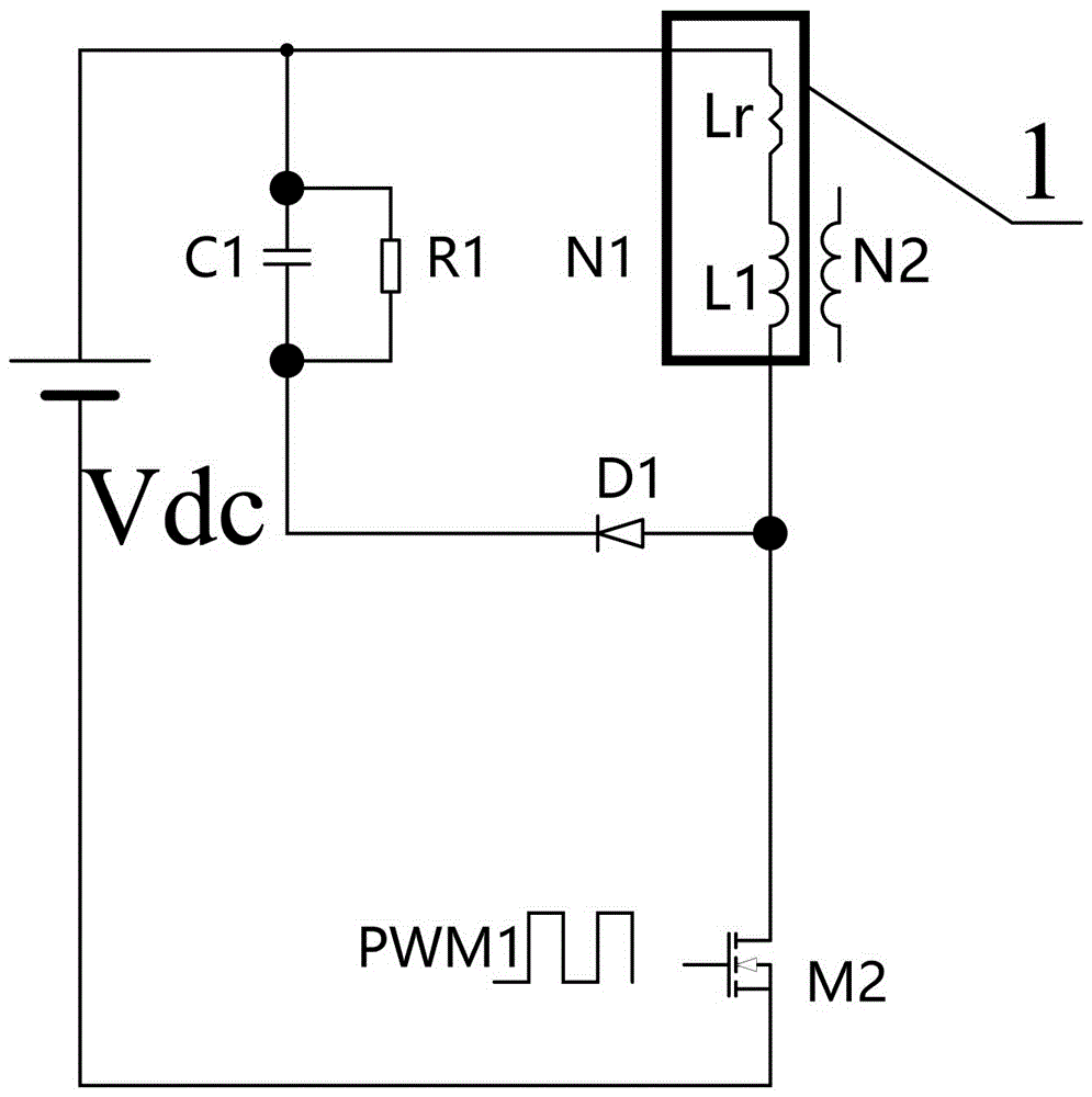
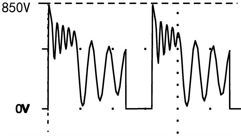
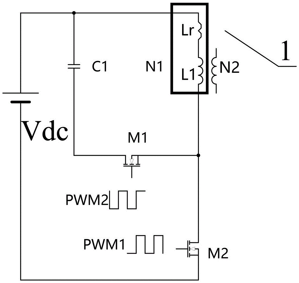
[0023] Please refer to Figure 4 The structure diagram of the first automatic clamping circuit of the first embodiment provided by the present invention is shown

[0024] This embodiment includes a cl...


PUM


Abstract

The invention relates to an automatic clamping circuit which comprises a clamping switch M1, a master power switch M2, a first diode D1, a second diode D2, a first resistor R1, a first capacitor C1 and a coil N1, when the clamping switch M1 is MOSFET, a grid electrode and a source electrode of the clamping switch M1 is respectively connected with a cathode and an anode of the first diode D1, and the grid electrode and a drain electrode are respectively connected with a cathode and an anode of the second diode D2; a drain electrode of the master power switch M2 is connected with a cathode of the first diode D1 in series, an anode of the first diode D1 is connected with the coil N1 in series, and the first resistor R1 is connected with the cathode and the anode of the first diode D1 in parallel to form an RD parallel circuit; the first capacitor C1 is connected with a drain electrode of the clamping switch M1 to form a series circuit, and the series circuit is connected with the coil N1 in parallel to form a closed circuit; the first capacitor Ci is controlled by the clamping switch M1 and is used for releasing and absorbing partial energy of the coil N1.

Description

technical field [0001] The invention relates to the technical field of switching power supplies, in particular to a switching converter with voltage clamping. Background technique [0002] At present, the main power switch M2 of the switching power supply generally uses a MOSFET or a triode. At the moment when the main power switch M2 is turned off, the leakage inductance causes a high peak voltage. The existing technology uses an RCD or a complex active clamping circuit to deal with it. For this peak voltage, the traditional RCD consumes this part of energy through resistance heating, which reduces the efficiency of the converter; the use of the existing active clamp is better than the RCD method, but because the drive of the clamp switch M1 is floating, Therefore, complex driving technology must be used to control the on and off of the clamp switch M1, so a complex and expensive IC is required, and the number of auxiliary devices is large, the cost is high and it is suscep...

Claims


Application Information

Patent Timeline
Patent Type & Authority Applications(China)
IPC IPC(8): H02M1/32
CPCH02M1/32H02M1/0038
Inventor 马丽娟
Owner 马丽娟
Why Eureka
Try Eureka