Differential charge pump circuit

A charge pump and circuit technology, applied in the direction of conversion equipment without intermediate conversion to AC, can solve the problems of change, large parasitic capacitance, charge loss control switch tube voltage, etc., achieve fast speed and reduce the effect of node parasitic capacitance

Pending Publication Date: 2017-09-19
CHENGDU ANALOG CIRCUIT TECH INC
View PDF7 Cites 0 Cited by
  • Summary
  • Abstract
  • Description
  • Claims
  • Application Information

AI Technical Summary

Problems solved by technology

The existing differential charge pump circuit often has large parasitic capacitance, more charge loss and changes in the control switch voltage, resulting in reduced output voltage, output current and conversion efficiency

Method used


Image

  • Differential charge pump circuit
  • Differential charge pump circuit

Examples


Embodiment Construction

[0013] The technical solution of the present invention will be further described in detail below in conjunction with the accompanying drawings, but the protection scope of the present invention is not limited to the following description.

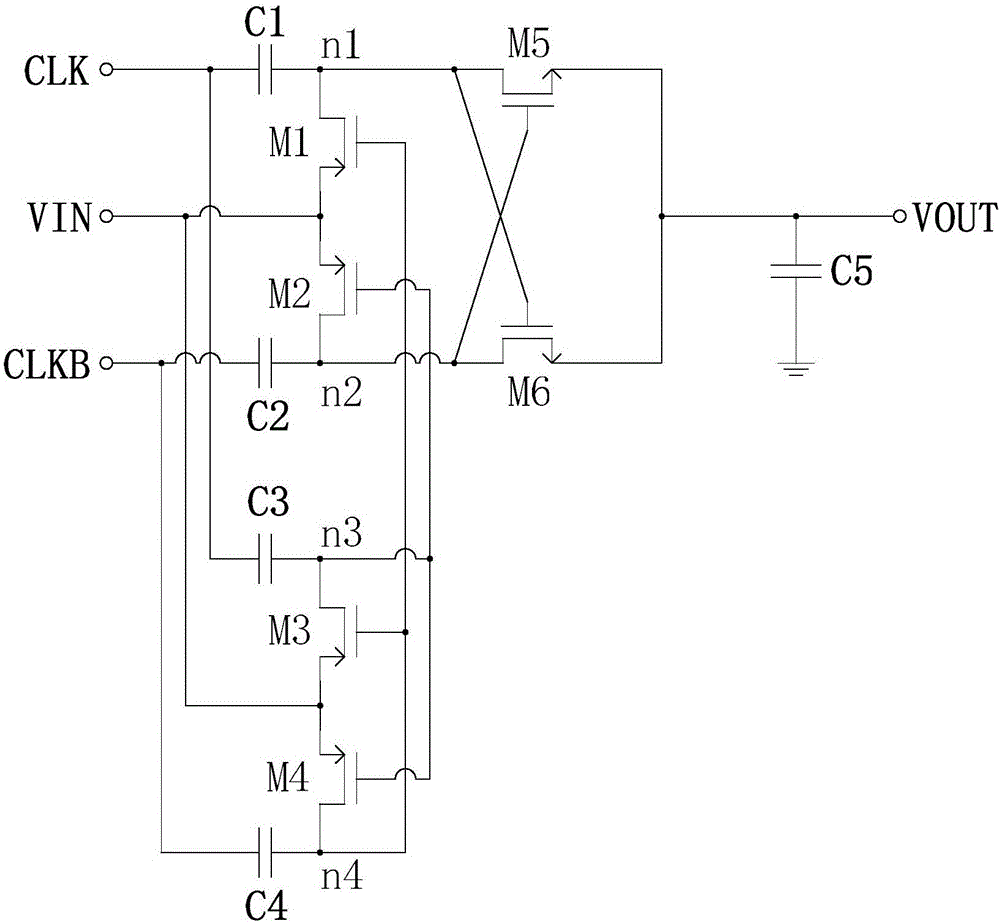
[0014] like figure 1 As shown, the differential charge pump circuit of the present invention includes an input voltage terminal VIN, a first clock signal input terminal CLK, a second clock signal input terminal CLKB, a first FET M1 connected to the input voltage terminal VIN, a second FET The transistor M2, the third field effect transistor M3 and the fourth field effect transistor M4, the first capacitor C1 and the third capacitor C3 connected to the first clock signal input terminal CLK, and the second capacitor connected to the second clock signal input terminal CLKB C2 and the fourth capacitor C4, the fifth field effect transistor M5 connected to the first capacitor C1, the sixth field effect transistor M6 connected to the second capaci...


PUM


Abstract

The invention discloses a differential charge pump circuit, which includes an input voltage end, a first clock signal input end, a second clock signal input end, first to fourth field effect transistors (FETs) connected separately with the input voltage end, first and third capacitors connected with the first clock signal input end, second and fourth capacitors connected with the second clock signal input end, a fifth FET, a sixth FET, an output capacitor and an output voltage end. The first clock signal input end and the second clock signal input end input a pair of differential clock signals. The differential charge pump circuit reduces the stray capacitance by driving gates of the first FET and the second FET and meanwhile, provides stable driving voltage for the fifth FET and the sixth FET to improve the output voltage of the output voltage end, the output current and the conversion efficiency. According to the invention, the higher voltage and current can be output and a higher conversion efficiency can be gained.

Description

technical field [0001] The invention relates to the field of integrated circuits, in particular to a differential charge pump circuit. Background technique [0002] Charge pump circuits are commonly used to generate an output voltage higher than the input voltage, or to provide negative voltages. The charge pump circuit has simple structure, small area and high efficiency. Now, how to improve the output voltage, output current and conversion efficiency is the development direction of the charge pump circuit design. [0003] Developed from the most basic charge pump circuit to a differential charge pump circuit, its current drive capability has been doubled. The existing differential charge pump circuit often has a large parasitic capacitance, a large loss of charge and a change in the voltage of the control switch tube, which reduces the output voltage, output current and conversion efficiency. Especially in the negative voltage charge pump circuit, if the first switch co...

Claims


Application Information

Patent Timeline
Patent Type & Authority Applications(China)
IPC IPC(8): H02M3/07
CPCH02M3/07
Inventor 何忠波
Owner CHENGDU ANALOG CIRCUIT TECH INC
Why Eureka
Try Eureka