Carrier storage enhanced super-junction IGBT (Insulated Gate Bipolar Transistor)
A gate structure and conductivity type technology, applied in the field of semiconductor power devices, can solve the problems of increasing on-voltage, weak storage effect, and weak carrier storage effect, etc.
- Summary
- Abstract
- Description
- Claims
- Application Information
AI Technical Summary
Problems solved by technology
Method used
Image

Examples
Embodiment Construction
[0090] The present invention will be described in detail below in conjunction with the accompanying drawings.
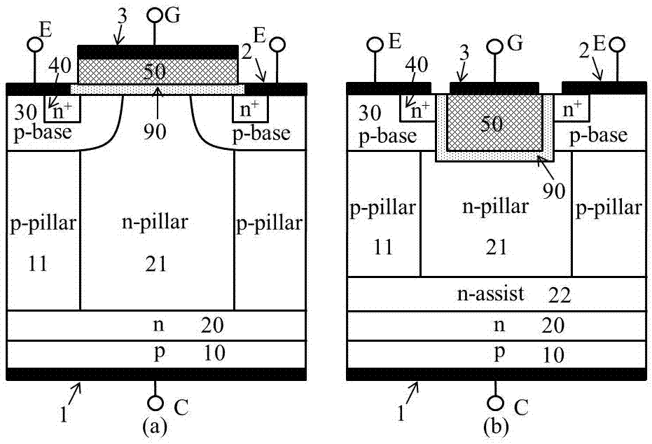
[0091] figure 1 (a) shows the schematic diagram of the traditional super-junction planar gate IGBT structure, figure 1 (b) shows the schematic diagram of the conventional semi-superjunction trench-gate IGBT. The main difference between the semi-superjunction IGBT and the superjunction IGBT is that there is an n-assist region 22 of an auxiliary layer between the n-column region 21 and the p-column region 11 and the buffer zone 20 to withstand the applied voltage. exist figure 1 (a) and figure 1 In (b), when the IGBT is forward-conducting, the p-base region 30 of the base region and the PN junction formed by the p-column region 11 and the n-column region 21 are reverse-biased, so the minority carriers in the n-column region 21 are close to the base The carrier concentration near the p-base region 30 and the p-pillar region 11 is relatively low, and the voltage drop...
PUM
 Abstract
Description
Claims
Application Information