Grid scanning drive circuit and liquid crystal display device

A driving circuit, gate scanning technology, applied in static indicators, nonlinear optics, instruments, etc., can solve problems such as the negative impact of thin film transistors, and achieve the effect of improving repairability and adding auxiliary repair modules

Active Publication Date: 2017-09-29
NANJING CEC PANDA LCD TECH
View PDF3 Cites 16 Cited by
  • Summary
  • Abstract
  • Description
  • Claims
  • Application Information

AI Technical Summary

Problems solved by technology

[0004] In order to solve the above technical problems, the present invention provides a gate scanning drive circuit, which can solve the problem of negative impact on thin film transistors caused by maintaining the module for a long time operation, and the reliability of the circuit can be improved by adopting a special step-by-step module design

Method used


Image

  • Grid scanning drive circuit and liquid crystal display device
  • Grid scanning drive circuit and liquid crystal display device
  • Grid scanning drive circuit and liquid crystal display device

Examples


Embodiment 1

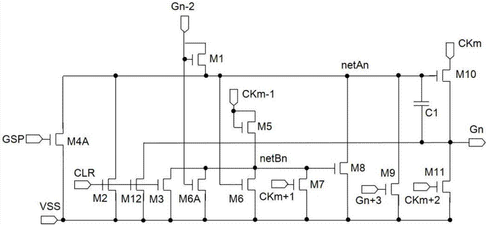
[0063] figure 2 It is a schematic circuit diagram of Embodiment 1 of a gate scanning drive circuit of the present invention, as shown in figure 2 As shown, a gate scanning driving circuit includes a multi-level gate driving unit, each gate driving unit includes: a pull-up control module 01, a pull-up module 03, a pull-down clearing module 04, and a main maintenance module 05; The main maintenance module 05 includes a maintenance control node generation module and a node maintenance module connected thereto; both the pull-up control module 01 and the maintenance control node generation module are connected to the first front-end signal; the pull-up module 03 is connected to the current-level scanning signal line Gn ; Pull-down clearing module 04 is connected to the rear level signal; pull-up control module 01, pull-up module 03 and pull-down clearing module 04 are all connected to the pull-up control node netAn; maintain the control node to generate module input low level VSS...

Embodiment 2

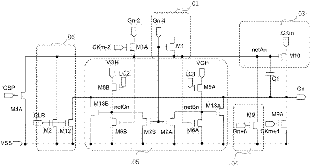
[0088] image 3 It is a schematic circuit diagram of Embodiment 2 of a gate scanning driving circuit of the present invention, as shown in image 3 As shown, the circuit composition structure of the second embodiment is basically the same as that of the first embodiment above, and does not include the stage transmission module 02 and the stage transmission signal maintenance module 053. The node maintenance control module further includes a pull-up control node maintenance module for maintaining the pull-up control node netAn, the pull-up control node maintenance module includes an eighth thin film transistor M8A and an eighteenth thin film transistor M8B, and the eighth thin film transistor The gate of M8A is connected to the first maintenance control point netBn, the source of the eighth thin film transistor M8A is connected to the pull-up control node netAn, the drain of the eighth thin film transistor M8A is connected to the low level VSS, the eighteenth thin film transist...

Embodiment 3

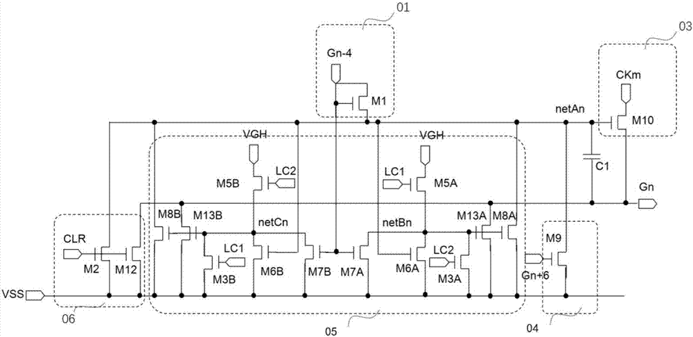
[0093] Figure 4 It is a schematic circuit diagram of Embodiment 3 of a gate scanning driving circuit of the present invention, as shown in Figure 4 As shown, the circuit composition structure of the third embodiment is basically the same as that of the second embodiment above, and does not include the stage transmission module 02 and the stage transmission signal maintenance module 053. The nineteenth thin film transistor M1A and the twentieth thin film transistor M4A can be set as functional modules that assist in maintaining the pull-up control node netAn.

[0094] The gate of the nineteenth thin film transistor M1A is connected to the front stage clock signal CKm-2, the source of the nineteenth thin film transistor M1A is connected to the second front stage signal, and the drain of the nineteenth thin film transistor M1A is connected to the pull-up control node net An.

[0095] The gate of the twentieth TFT M4A is connected to the start signal GSP, the source of the twe...


PUM


Abstract

The invention discloses a grid scanning drive circuit comprising multiple grid drive units. Each grid drive unit comprises a pull-up control module, a pull-up module, a pull-down emptying module and a main maintenance module. The main maintenance module comprises a maintenance control node generation module and a node maintenance module which is connected with the maintenance control node generation module. The maintenance control node generation module comprises a first child maintenance control node generation module and a second child maintenance control node generation module which are symmetrical. The first child maintenance control node generation module inputs a first low frequency clock signal. The second child maintenance control node generation module inputs a second low frequency clock signal opposite to the first low frequency clock signal. The first child maintenance control node generation module and the second child maintenance control node generation module alternately work under the control of the first low frequency clock signal and the second low frequency clock signal. The adverse impact on the thin-film transistor caused by long-term operation of the maintenance module can be effectively avoided.

Description

technical field [0001] The invention relates to the technical field of liquid crystal display, in particular to a grid scanning driving circuit and a liquid crystal display device. Background technique [0002] Due to the requirements of narrow bezel applications of liquid crystal displays, the current mainstream technology is to directly integrate the scanning line driving function in the original gate IC (gate IC) on the array substrate of the liquid crystal display, using the existing thin film transistor manufacturing process Make a gate scanning circuit with shift register function. Recently, more and more large-size TVs use this technology, and this puts forward higher requirements for the design of the gate scanning circuit, whether it is the reliability of the circuit or the yield of production. [0003] Such as figure 1 Shown is the gate scanning drive circuit design currently used in product design. The gate scan drive circuit mainly includes a pull-up control mo...

Claims


Application Information

Patent Timeline
Patent Type & Authority Applications(China)
IPC IPC(8): G09G3/36
CPCG09G3/3677G09G2310/0286G02F1/136286G02F1/1368
Inventor 戴超
Owner NANJING CEC PANDA LCD TECH
Why Eureka
Try Eureka