A class of organic transistor storage electret material and its preparation method and application
A technology of organic transistors and electrets, which is applied to the application of materials in the field of electric storage of organic transistors, and the field of preparation and synthesis of charge storage materials, can solve the problems that have been explored, and achieve enhanced solubility, mild reaction conditions, and low toxicity. Effect
- Summary
- Abstract
- Description
- Claims
- Application Information
AI Technical Summary
Problems solved by technology
Method used
Image
Examples
example
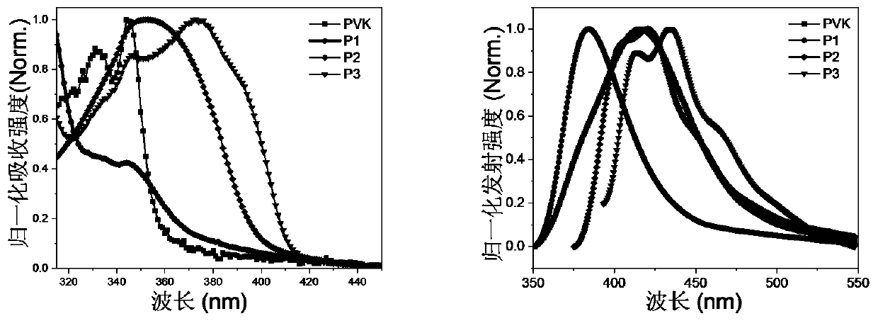
[0041] Example implementation 2, THF:Tol=1:1 solvent 80mL is placed in a 100mL Erlenmeyer flask, DC8BrF (1.6g, 3.42mmol) is dissolved in this organic solvent; newly configured K2 CO 3 / KF (2M) aqueous solution was also placed in another 100mL Erlenmeyer flask, and both were bubbled to remove oxygen for 2h. DBC8OPFOH (1g, 1.57mmol) and bis(triphenylphosphine)palladium dichloride (0.22g, 0.314mmol) were added to a dry two-necked flask. Inject the DC8BrF solution into the two-necked bottle under N2 atmosphere, raise the temperature to 90°C, and inject K 2 CO 3 / KF (2M) aqueous solution 5mL. After reacting for 48 hours, it was detected that the reaction was complete, quenched by adding water, extracted with dichloromethane several times, combined the oil phases and dried over anhydrous sodium sulfate. Column chromatography used petroleum ether: dichloromethane = 3:1 as eluent to obtain light yellow Oily product 1.2 g (61% yield). 1 H NMR (400MHz, CDCl 3 ,δ):7.81(d,J=8.0Hz,2H...
Embodiment 7
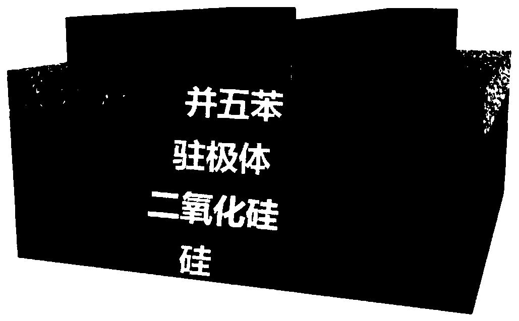
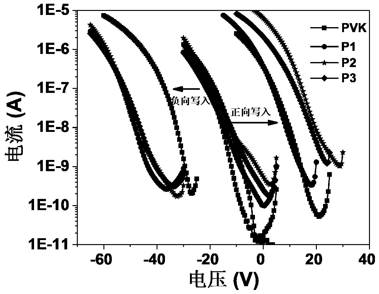
[0050] Implementation example 7, the present invention provides a method for preparing a transistor storage device, the device is prepared on a heavily doped n-type silicon wafer, and the 300nm thick SiO grown on the Si wafer 2 as a gate insulating layer. Si / SiO 2 The substrates were ultrasonically cleaned in toluene, acetone, and ethanol for 20 minutes, and finally the substrates were cleaned with deionized water, and then dried in an oven at 80°C for 30 minutes. The toluene solutions of PVK, P1, P2 and P3 were spin-coated on the substrate to form a 20nm thick film, and the corresponding concentrations of each solution were 8mgmL -1 , 6mgmL -1 , 5mgmL -1 and 8mgmL -1 . These spun-on substrates were then placed in an oven at 80°C for 30 min. Then take out the silicon wafer and put it on the mask plate and put it into the vacuum evaporation table, and heat the evaporation table in stages until the work is stable, at a pressure of 5×10 -4 Pa, deposition rate Pentacene w...
PUM
 Abstract
Description
Claims
Application Information
 - R&D
- Intellectual Property
- Life Sciences
- Materials
- Tech Scout
- Unparalleled Data Quality
- Higher Quality Content
- 60% Fewer Hallucinations
Browse by: Latest US Patents, China's latest patents, Technical Efficacy Thesaurus, Application Domain, Technology Topic, Popular Technical Reports.
© 2025 PatSnap. All rights reserved.Legal|Privacy policy|Modern Slavery Act Transparency Statement|Sitemap|About US| Contact US: help@patsnap.com


