Novel method and device for carrying out micro electrical discharge machining on thin-sheet microelectrode array

A processing method and micro-electrode technology, which are applied in electric processing equipment, electrode manufacturing, metal processing equipment, etc., can solve problems such as the adverse effect of the shape accuracy of three-dimensional microstructures, the adverse effect of the shape accuracy of plane features, etc., so as to eliminate the step effect and improve the The effect of precision

Active Publication Date: 2017-10-13
SHENZHEN UNIV
View PDF6 Cites 6 Cited by
  • Summary
  • Abstract
  • Description
  • Claims
  • Application Information

AI Technical Summary

Problems solved by technology

However, there are the following problems in the process of implementation: ① When the microelectrode micro-EDM surface features are processed by the thin slice array, there will be steps on the surface of the obtained three-dimensional microstructure, and the steps will have an adverse effect on the shape accuracy of the three-dimensional microstructure; When micro-electrode micro-EDM plane features, rounded discharge marks will appear on the surface of the planar features, and the rounded discharge marks will adversely affect the shape accuracy of the planar features

Method used


Image

  • Novel method and device for carrying out micro electrical discharge machining on thin-sheet microelectrode array
  • Novel method and device for carrying out micro electrical discharge machining on thin-sheet microelectrode array
  • Novel method and device for carrying out micro electrical discharge machining on thin-sheet microelectrode array

Examples


Embodiment Construction

[0037] It should be understood that the specific embodiments described here are only used to explain the present invention, not to limit the present invention.

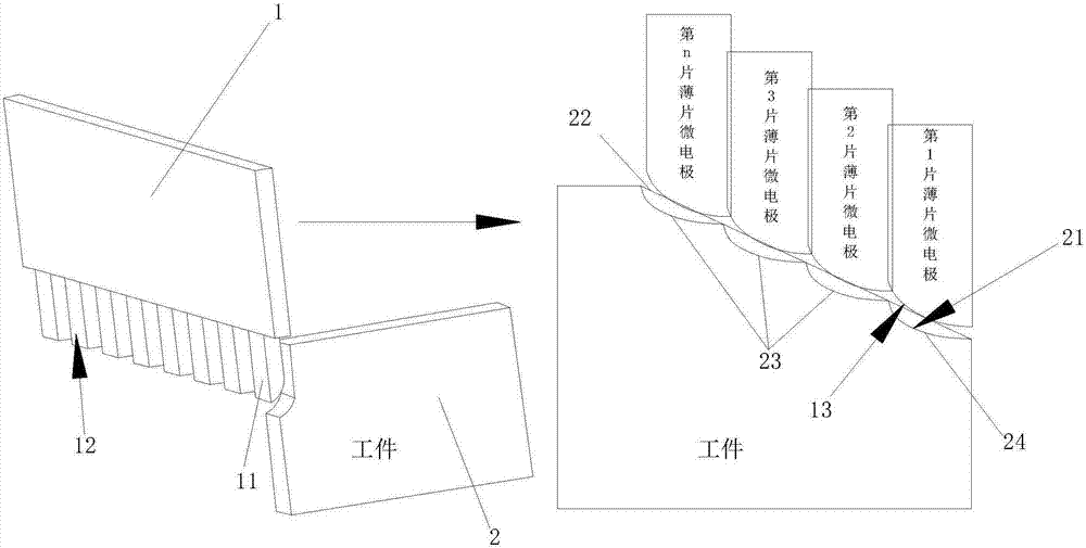
[0038] refer to figure 1 and Figure 5 , the present invention discloses an embodiment of a thin-sheet array microelectrode 1 micro-electric discharge machining method. The sheet array microelectrode 1 includes a plurality of sheet microelectrodes 12 arranged in sequence. Under the influence of the skin effect, the thickness of the sheet microelectrodes 12 The processed end face 13 is lost to a convex arc shape.

[0039] refer to figure 1 , thin sheet array microelectrode 1 micro electric discharge machining method includes:

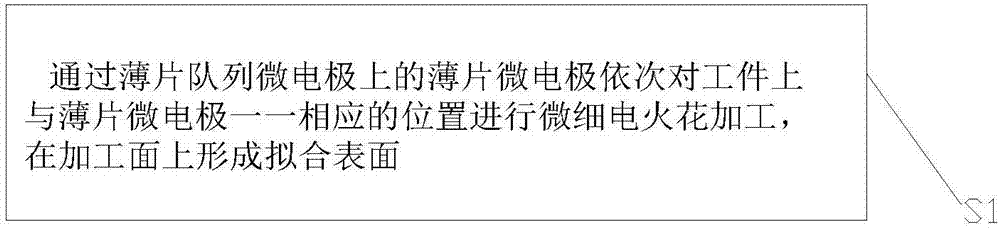
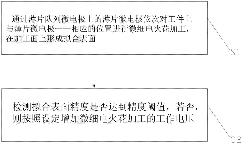
[0040] S1. Using the thin sheet microelectrodes 12 on the thin sheet array microelectrodes 1, perform micro-EDM on the corresponding positions of the thin sheet microelectrodes 12 on the workpiece 2 in order to form a fitting surface 21 on the processing surface.

[0041] In the above-mentio...


PUM

PropertyMeasurementUnit
thicknessaaaaaaaaaa
thicknessaaaaaaaaaa
thicknessaaaaaaaaaa

Abstract

The invention discloses a novel method and device for carrying out electrical discharge machining on a thin-sheet microelectrode array. The thin-sheet microelectrode array comprises a plurality of thin-sheet microelectrodes which are arrayed in sequence, and machining end faces of the thin-sheet microelectrodes are worn to form convex arc shapes under the influence of the skin effect. The novel method for carrying out the micro electrical discharge machining on the thin-sheet microelectrode array comprises the step of carrying out the micro electrical discharge machining on the positions, corresponding to the thin-sheet microelectrodes in a one-to-one mode, on a workpiece through the thin-sheet microelectrodes of the thin-sheet microelectrode array to form a fitting surface on the machined surfaces. According to the novel method for carrying out the micro electrical discharge machining on the thin-sheet microelectrode array, the characteristic of the filleted corner wear of the machining end faces of conventional thin-sheet microelectrodes is fully utilized to effectively eliminate the step effect of the fitting surface with a three-dimensional microstructure, so that the precision of the machined fitting surface is improved; and the step effect of the fitting surface with the three-dimensional microstructure and filleted corner discharge marks of the fitting surface with plane characteristics can be eliminated.

Description

technical field [0001] The invention relates to the field of electric discharge machining, in particular to a novel micro-electrode discharge processing method and device for sheet array micro-electrodes. Background technique [0002] The existing method of discretizing a three-dimensional microelectrode into several sheet array microelectrodes, and making the sheet array microelectrodes sequentially perform micro-electric discharge machining according to a planned path can obtain a three-dimensional microstructure. However, there are the following problems in the process of implementation: ① When the microelectrode micro-EDM surface features are processed by the thin slice array, there will be steps on the surface of the obtained three-dimensional microstructure, and the steps will have an adverse effect on the shape accuracy of the three-dimensional microstructure; When microelectrode micro-EDM plane features, rounded discharge marks will appear on the surface of the plana...

Claims


Application Information

Patent Timeline
Patent Type & Authority Applications(China)
IPC IPC(8): B23H1/00B23H1/04
CPCB23H1/00B23H1/04
Inventor 徐斌伍晓宇雷建国梁雄赵航程蓉郭登极阮双琛
Owner SHENZHEN UNIV
Why Eureka
Try Eureka