Display panel, making method and display device

A technology of a display panel and a manufacturing method, applied in the field of display panels, manufacturing methods and display devices, can solve the problems of adverse effects of resin material performance, influence on performance of display panels, increase of manufacturing time, etc., so as to shorten the manufacturing time, avoid adverse effects, Avoiding the effect of threshold voltage drift

Active Publication Date: 2017-10-13
BOE TECH GRP CO LTD
View PDF9 Cites 15 Cited by
  • Summary
  • Abstract
  • Description
  • Claims
  • Application Information

AI Technical Summary

Problems solved by technology

However, since the annealing process is an additional step in the display panel manufacturing process, it will lead to an increase in production time and a decrease in production capacity
In addition, the annealing process will also adversely affect the performance of the resin material, which will also affect the performance of the display panel

Method used


Image

  • Display panel, making method and display device
  • Display panel, making method and display device
  • Display panel, making method and display device

Examples


Embodiment 1

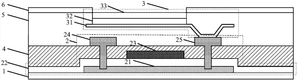
[0032] Such as figure 1 As shown, this embodiment provides a display panel, including a base substrate 1 , a thin film transistor 2 formed on the base substrate 1 , and a light emitting structure 3 formed on the side of the thin film transistor 2 facing away from the base substrate 1 . Wherein, the thin film transistor 2 includes a polysilicon layer 21 located between the light emitting structure 3 and the base substrate 1 . A light-shielding layer 4 for blocking ultraviolet light is also formed between the polysilicon layer 21 and the light-emitting structure 3 . The orthographic projection of the light-shielding layer 4 on the base substrate 1 covers the orthographic projection of the polysilicon layer 21 on the base substrate 1 .

[0033] It can be understood that the light emitting structure 3 may specifically include an anode 31 , a light emitting layer 32 and a cathode 33 , wherein the anode 31 is electrically connected to the thin film transistor 2 . After the anode 31...

Embodiment 2

[0046] This embodiment provides a method for manufacturing a display panel, and the method for manufacturing a display panel is applied to the display panel described in Embodiment 1.

[0047] Such as Figure 5 As shown, the manufacturing method of the display panel specifically includes:

[0048] Step S1: providing a base substrate.

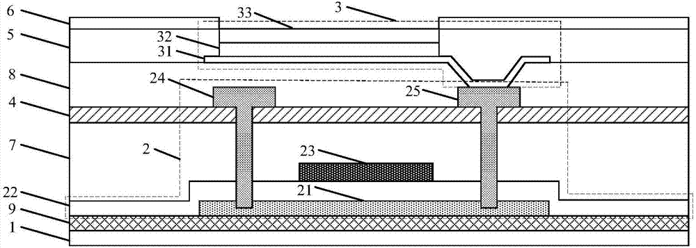
[0049] Step S2: forming a thin film transistor and a light-shielding layer for blocking ultraviolet light on the base substrate, so that the thin film transistor includes a polysilicon layer; the light-shielding layer is located on the side of the polysilicon layer facing away from the base substrate, and the light-shielding layer is projected on the front of the base substrate Orthographic projection of the covering polysilicon layer on the base substrate.

[0050] Step S3: forming a light-emitting structure on the side of the light-shielding layer facing away from the polysilicon layer.

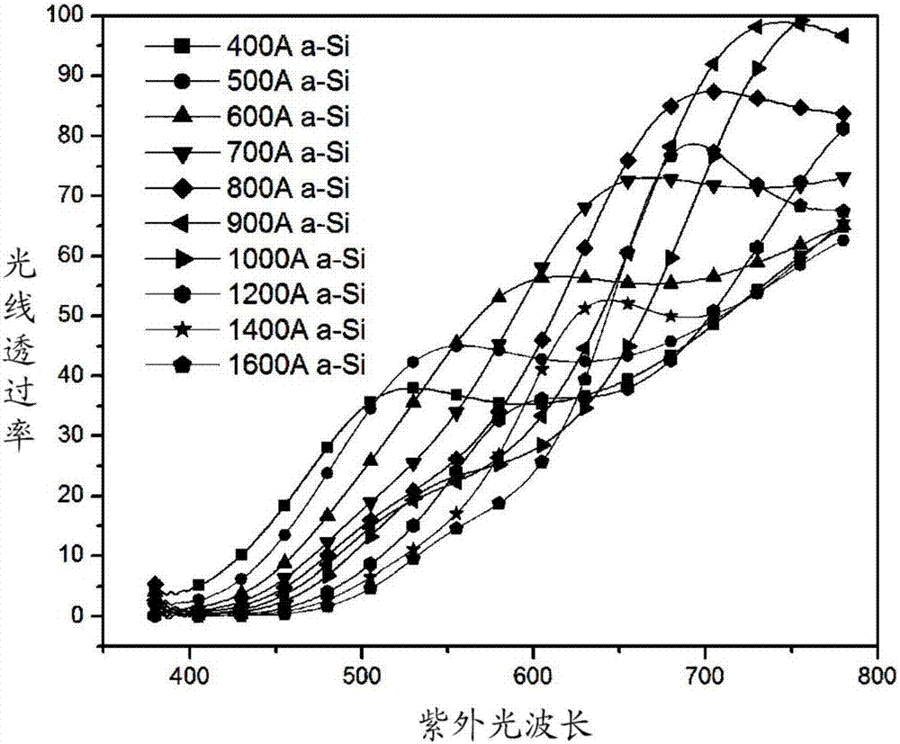
[0051] Using the manufacturing method of the display...

Embodiment 3

[0065] This embodiment provides a display device, and the display device includes the display panel as described in the first embodiment.

[0066] Since the display device provided in this embodiment includes the display panel as described in Embodiment 1, the display device can avoid the adverse effect of ultraviolet light on the polysilicon layer, thereby avoiding the problem of threshold voltage shift of the thin film transistor. Moreover, since no additional annealing process is required, the manufacturing time of the display device is shortened and the production capacity is improved.


PUM


Abstract

The invention provides a display panel, a making method and a display device and relates to the technical field of display. The problem of threshold voltage drift of a thin film transistor caused by the fact that ultraviolet generates adverse influence on a polycrystalline silicon layer can be avoided. The display panel comprises a substrate baseplate, a thin film transistor formed on the substrate baseplate and a luminous structure formed on one side, back on to the substrate baseplate, of the thin film transistor, the thin film transistor comprises a polycrystalline silicone layer positioned between the luminous structure and the substrate baseplate, a light shielding layer for blocking ultraviolet is formed between the polycrystalline silicon layer and the luminous structure, and orthographic projection of the light shielding layer on the substrate baseplate covers that of the polycrystalline silicon layer on the substrate baseplate. The display panel is used for realizing picture display.

Description

technical field [0001] The present invention relates to the field of display technology, in particular to a display panel, a manufacturing method, and a display device. Background technique [0002] In a display panel based on LTPS (Low temperature polysilicon technology, low temperature polysilicon technology), it includes a base substrate, a thin film transistor formed on the base substrate, a pixel defining layer, a spacer and a light emitting structure. Wherein, the pixel defining layer and the spacer can be manufactured separately, or can be manufactured simultaneously by using an HT (Half Tone, half tone) process. [0003] In the manufacturing process of the display panel, the pixel defining layer and the spacer are formed after the formation of the thin film transistor and the anode in the light-emitting structure. However, since the light-emitting layer in the light-emitting structure needs to be formed , it is necessary to perform ultraviolet light exposure treatme...

Claims


Application Information

Patent Timeline
Patent Type & Authority Applications(China)
IPC IPC(8): G09F9/00H01L27/12
CPCG09F9/00H01L27/1248H01L29/66757H01L29/78633H01L29/78675H01L27/1222H01L29/42384H01L29/41733
Inventor 姚琪曹占锋张锋李海旭班圣光刘志勇
Owner BOE TECH GRP CO LTD
Why Eureka
Try Eureka