
Liquid crystal display panel and driving method thereof

A technology of liquid crystal display panels and thin film transistors, applied in static indicators, nonlinear optics, instruments, etc., can solve the problems of loss of pixel aperture ratio, influence of back-end process yield, and increase of production costs

Inactive Publication Date: 2017-10-24
SHENZHEN CHINA STAR OPTOELECTRONICS TECH CO LTD
View PDF3 Cites 3 Cited by
  • Summary
  • Abstract
  • Description
  • Claims
  • Application Information

AI Technical Summary

Problems solved by technology

However, increasing the line width of scanning lines and data lines will lose the aperture ratio of pixels and reduce the penetration rate of liquid crystal panels; increasing the film thickness of scanning lines and data lines will increase production costs and have a certain impact on the yield of the back-end process. influences

Method used


Image

  • Liquid crystal display panel and driving method thereof
  • Liquid crystal display panel and driving method thereof
  • Liquid crystal display panel and driving method thereof

Examples


Embodiment Construction

[0021] The following will clearly and completely describe the technical solutions in the embodiments of the present invention with reference to the drawings in the embodiments of the present invention. Wherein, the accompanying drawings are only used for exemplary illustration, and represent only schematic diagrams, and should not be understood as limitations on this patent.

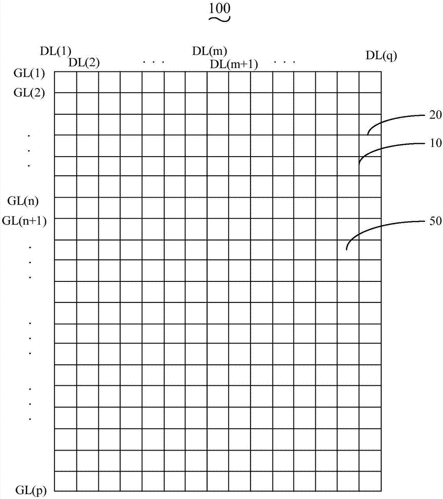
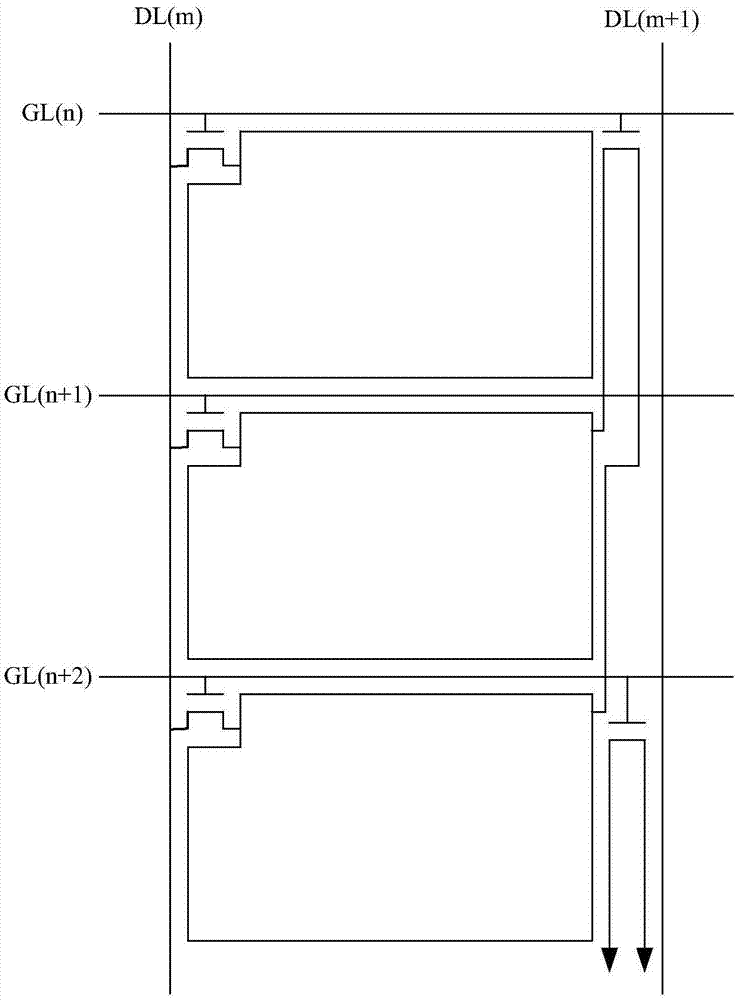
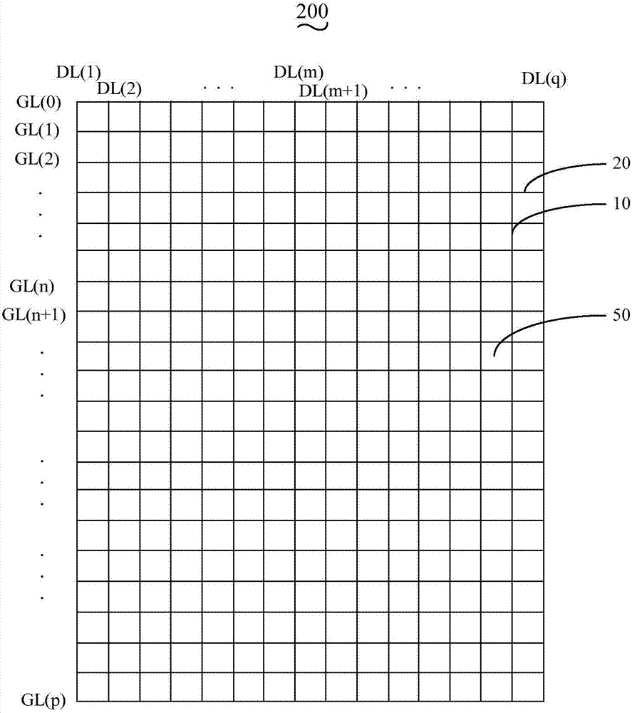
[0022] Please also refer to figure 1 and figure 2 , the present invention provides a liquid crystal display panel 100 . The liquid crystal display panel 100 includes an array substrate, a color filter substrate and a liquid crystal layer. The array substrate is opposite to the color filter substrate and arranged in parallel with each other, and the liquid crystal layer is located between the array substrate and the color filter substrate. A common electrode layer is stacked on the side of the color filter substrate facing the liquid crystal layer, the common electrode layer includes a plurality of co...


PUM


Abstract

The invention provides a liquid crystal display panel. One second thin film transistor is added in a scanning line between two adjacent first thin film transistors in a scanning line in each odd-numbered row or a scanning line in an even-numbered row. A source electrode and a leak electrode of a second thin film transistor in the nth row are respectively and electrically connected to pixel electrodes which are electrically connected with thin film transistors in the n+1 row and the n+2 row. The pixel electrodes are electrically connected with the second thin film transistor and the thin film transistors. Before the pixel electrodes are charged, charge neutrality is carried out on the pixel electrodes by the second thin film transistor such that voltage required by the pixel electrodes is lowered. The pixel electrodes are electrically connected to the thin film transistors and the second thin film transistor. Therefore, the liquid crystal panel is charged in the short time, thereby improving image quality and reliability of the liquid crystal panel.

Description

technical field [0001] The invention relates to the field of display technology, in particular to a liquid crystal display panel and a driving method thereof. Background technique [0002] As the size of the liquid crystal panel increases and the resolution becomes higher and higher, the turn-on time of each scanning line will be further compressed. For example, the pixels of FHD (Full High Definition, Full HD) panels are 1920×1080), and when the screen refresh rate is 60Hz, the turn-on time of each scan line is about 1 / (60*1080)≈15.4ms; The UHD (Ultra High Definition, Ultra High Definition) panel generally has a resolution of 3840×2160. When the screen refresh rate is 60Hz, the turn-on time of each scan line is about 1 / (60*2160)≈7.7ms. Since the turn-on time of the scanning line is compressed due to the increase in resolution, it may cause insufficient charging of the liquid crystal panel, thereby reducing the display effect of the image. In the prior art, a common soluti...

Claims


Application Information

Patent Timeline
IPC IPC(8): G02F1/1362G02F1/1368G02F1/133
CPCG02F1/136227G02F1/13306G02F1/1368
Inventor 陈帅
Owner SHENZHEN CHINA STAR OPTOELECTRONICS TECH CO LTD
Learn More