OLED display panel and its preparation method

A technology for display panels and array substrates, which is applied in the manufacture of semiconductor/solid-state devices, semiconductor devices, electrical components, etc., can solve problems such as crosstalk, increased lateral current of display panels, and reduced display quality of OLED display panels, and eliminates light leakage. , the effect of improving the display quality

Active Publication Date: 2020-09-15
WUHAN CHINA STAR OPTOELECTRONICS SEMICON DISPLAY TECH CO LTD
View PDF7 Cites 0 Cited by
  • Summary
  • Abstract
  • Description
  • Claims
  • Application Information

AI Technical Summary

Problems solved by technology

When the pitch of light-emitting units is reduced and the transmission performance of the first common layer is continuously improved, the lateral current of the display panel also increases, resulting in crosstalk
Specifically, in the structure of the existing OLED display panel as described above, since the first common layer of adjacent light-emitting units is connected, when one of the light-emitting units (the target light-emitting unit) is turned on, a small amount of holes can pass through the first common layer. A common layer is injected into the adjacent light-emitting unit, recombines with electrons in the adjacent light-emitting unit and then emits light, which leads to impure light emission of the target light-emitting unit. This light-emitting phenomenon is called leakage light-emitting phenomenon, and a small amount of holes leak The resulting current is called leakage current
Especially when the target light-emitting unit is lighted at low current, since the light emitted by the target light-emitting unit is also weak, the light leakage phenomenon is more obvious at this time, thereby reducing the display quality of the OLED display panel

Method used


Image

  • OLED display panel and its preparation method
  • OLED display panel and its preparation method
  • OLED display panel and its preparation method

Examples


Embodiment Construction

[0028] In order to make the object, technical solution and advantages of the present invention clearer, the specific implementation manners of the present invention will be described in detail below in conjunction with the accompanying drawings. Examples of these preferred embodiments are illustrated in the accompanying drawings. The embodiments of the invention shown in and described with reference to the drawings are merely exemplary, and the invention is not limited to these embodiments.

[0029] Here, it should also be noted that, in order to avoid obscuring the present invention due to unnecessary details, only the structures and / or processing steps closely related to the solution according to the present invention are shown in the drawings, and the related Other details are not relevant to the invention.

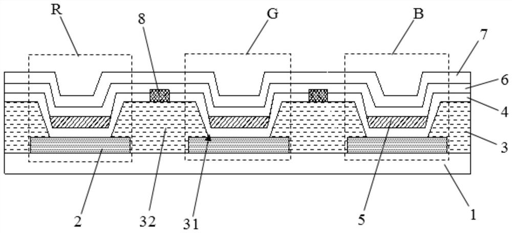
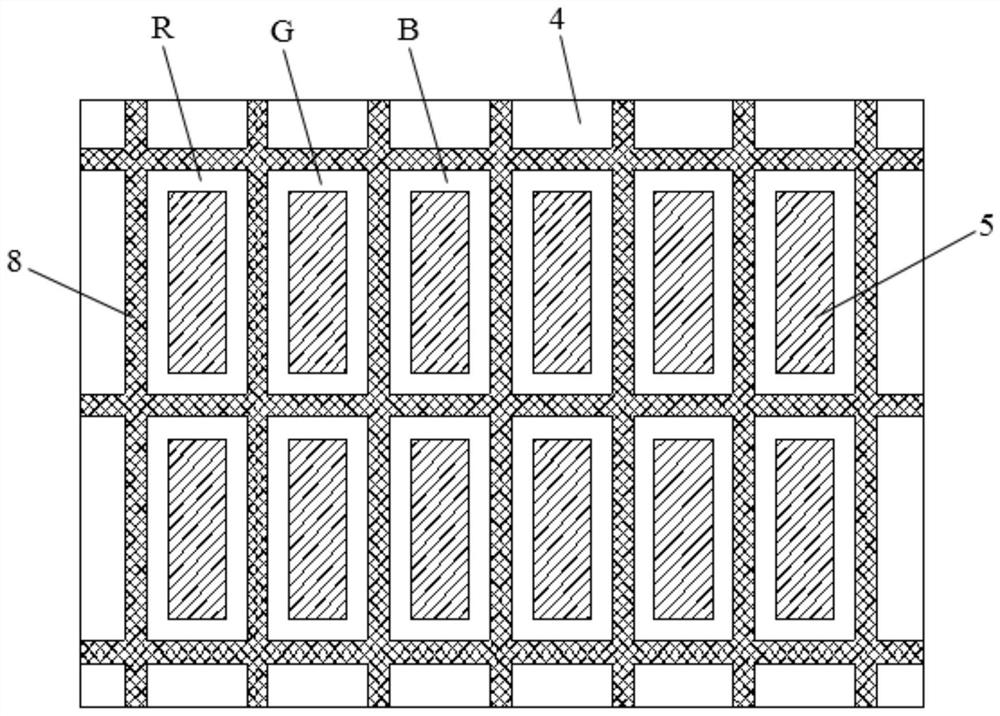
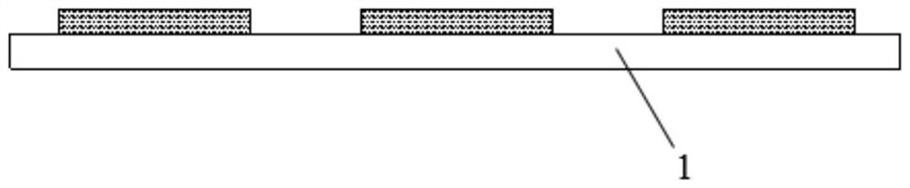
[0030] This embodiment firstly provides an OLED display panel, such as figure 1 As shown, the OLED display panel includes a TFT array substrate 1 and a plurality of ...


PUM


Abstract

The invention discloses an OLED display panel, which comprises a TFT array substrate and a plurality of anodes arrayed on the TFT array substrate. A pixel definition layer is arranged on the TFT array substrate, and the pixel definition layer includes the exposed The opening of the anode and the spacer for separating two adjacent anodes, each of the openings corresponds to a sub-pixel area; wherein, the pixel definition layer is sequentially provided with first holes for transporting holes. A common layer, a second common layer for transporting electrons, and a cathode layer, a luminescent material is respectively arranged between the first common layer and the second common layer corresponding to each sub-pixel area; wherein, the interval A hole blocking portion is further provided above the portion, and the hole blocking portion separates the first common layer between two adjacent sub-pixel regions from each other. The invention also discloses a preparation method of the above-mentioned OLED display panel.

Description

technical field [0001] The invention relates to the technical field of displays, in particular to an OLED display panel and a preparation method thereof. Background technique [0002] OLED (Organic Electroluminescent Diode) display devices have the characteristics of self-illumination, wide viewing angle, high luminous efficiency, low power consumption, fast response time, good low temperature characteristics, simple manufacturing process, and low cost, and have been widely used in the display field. [0003] The core component of an OLED display device is an OLED display panel. The structure of an OLED display panel generally includes: a TFT array substrate and an anode layer sequentially fabricated on the TFT substrate, a pixel definition layer, a first common layer, a light emitting layer, a second common layer and cathode layer. The anode layer includes a plurality of anodes arranged in an array, and the pixel definition layer includes a plurality of pixel openings that...

Claims


Application Information

Patent Timeline
Patent Type & Authority Patents(China)
IPC IPC(8): H01L27/32H01L51/56
CPCH10K59/126H10K59/122H10K59/1201H10K71/00
Inventor 杨杰张明
Owner WUHAN CHINA STAR OPTOELECTRONICS SEMICON DISPLAY TECH CO LTD
Why Eureka
Try Eureka