Array substrate, preparation method for array substrate, and display apparatus

A technology of array substrates and base substrates, applied in the direction of instruments, semiconductor devices, computing, etc., can solve problems such as contact short circuit, data line 10 is easy to break, and is defective

Inactive Publication Date: 2017-10-27
BOE TECH GRP CO LTD +1
View PDF4 Cites 8 Cited by
  • Summary
  • Abstract
  • Description
  • Claims
  • Application Information

AI Technical Summary

Problems solved by technology

[0004] However, for high-resolution (Pixels Per Inch, PPI for short) touch products, since the width of the space (Space) between the touch signal line 20 and the data line 10 is very small, the touch signal line 20 and the data line During the exposure process of the line 10, the problem of underexposure at the gap between the touch signal line 20 and the data line 10 often occurs
When the photoresist is a positive photoresist, if the exposure is insufficient, the etching between the touch signal line 20 and the data line 10 will not be clean, which will cause the data line 10 and the adjacent touch signal line 20 to contact and short circuit ( short), resulting in defects; but if overexposure (expanding the exposure area), it will lead to the formation of thinner data lines 10 and touch signal lines 20, so that in the fanout (fan-out) area because the data lines 10 are thinner, thus It will cause the data line 10 to be easily broken, thereby affecting the normal light emission of a column of pixels connected to the broken data line

Method used


Image

  • Array substrate, preparation method for array substrate, and display apparatus
  • Array substrate, preparation method for array substrate, and display apparatus
  • Array substrate, preparation method for array substrate, and display apparatus

Examples


Embodiment Construction

[0033] The following will clearly and completely describe the technical solutions in the embodiments of the present invention with reference to the accompanying drawings in the embodiments of the present invention. Obviously, the described embodiments are only some, not all, embodiments of the present invention. Based on the embodiments of the present invention, all other embodiments obtained by persons of ordinary skill in the art without making creative efforts belong to the protection scope of the present invention.

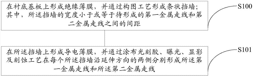
[0034] An embodiment of the present invention provides a method for preparing an array substrate, such as figure 2 shown, including:

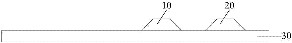
[0035] S100, such as image 3 As shown, an insulating film is formed on the base substrate 30, and a strip-shaped barrier wall 40 is formed through a patterning process; wherein, the width of the barrier wall 40 is less than or equal to the first metal wiring 10 and the second metal wiring 20 to be formed. spacing between. ...


PUM


Abstract

Embodiments of the invention provide an array substrate, a preparation method for the array substrate, and a display apparatus, and relate to the technical field of display. The exposure at a gap between a touch signal line and a data line can be enhanced. The method comprises the steps of forming an insulated film on a substrate and forming a strip-shaped retaining wall through a picture composition process, wherein the width of the retaining wall is smaller than or equal to a gap between to-be-formed first metal route and second metal route; and forming a conductive film on the retaining wall, and forming the first metal route and the second metal route on two sides of the retaining wall in an extension direction respectively through photoresist coating, exposure, development and etching processes. Therefore, the gap between the touch signal line and the data line can be fully exposed.

Description

technical field [0001] The present invention relates to the field of display technology, in particular to an array substrate, a preparation method thereof, and a display device. Background technique [0002] With the development of display technology, touch panel (Touch Panel) technology has entered a period of rapid development. According to the setting position of touch electrodes, touch panel can be divided into external touch panel and built-in touch panel. Control screen can be divided into: external touch screen (On cell Touch Panel) and embedded touch screen (In Cell Touch Panel). Among them, the InCell touch screen can be further divided into a hybrid in-cell (HIC for short) touch screen and a full in-cell (Full In Cell, FIC for short) touch screen. [0003] In order to reduce the thickness of the display screen, FIC touch products, in which a touch sensor (Touch Sensor) is built into a thin film transistor (TFT for short), have become the main development direction...

Claims


Application Information

Patent Timeline
Patent Type & Authority Applications(China)
IPC IPC(8): G06F3/041G02F1/1333
CPCG02F1/13338G06F3/0412G06F2203/04103H01L29/41733H01L27/124H01L27/1259G02F1/136286G02F1/1368G02F1/136295
Inventor 彭勇张鹏举李鑫
Owner BOE TECH GRP CO LTD
Why Eureka
Try Eureka