SOI MOSFET total dose radiation model building method

A technology of total dose irradiation and modeling method, which is applied in the field of intensive model modeling of devices, can solve the problems of wrong simulation results, affecting the effect of circuit evaluation, and the inability to simultaneously simulate NMOS and PMOS leakage current and threshold voltage drift, etc., to achieve Effects of Improving Simulation Accuracy

Active Publication Date: 2017-10-31
SHANGHAI INST OF MICROSYSTEM & INFORMATION TECH CHINESE ACAD OF SCI
View PDF7 Cites 5 Cited by
  • Summary
  • Abstract
  • Description
  • Claims
  • Application Information

AI Technical Summary

Problems solved by technology

[0007] In view of the above-mentioned shortcoming of prior art, the object of the present invention is to provide a kind of modeling method of SOI MOSFET total dose irradiation model, be used to solve the leakage problem that SOI total dose SPICE model can't simultaneously simulate NMOS and PMOS in the prior art. The magnitude of the current and threshold voltage drift will cause errors in the simulation results and affect the evaluation of the circuit, etc.

Method used


Image

  • SOI MOSFET total dose radiation model building method
  • SOI MOSFET total dose radiation model building method
  • SOI MOSFET total dose radiation model building method

Examples


Embodiment Construction

[0037] Embodiments of the present invention are described below through specific examples, and those skilled in the art can easily understand other advantages and effects of the present invention from the content disclosed in this specification. The present invention can also be implemented or applied through other different specific implementation modes, and various modifications or changes can be made to the details in this specification based on different viewpoints and applications without departing from the spirit of the present invention.

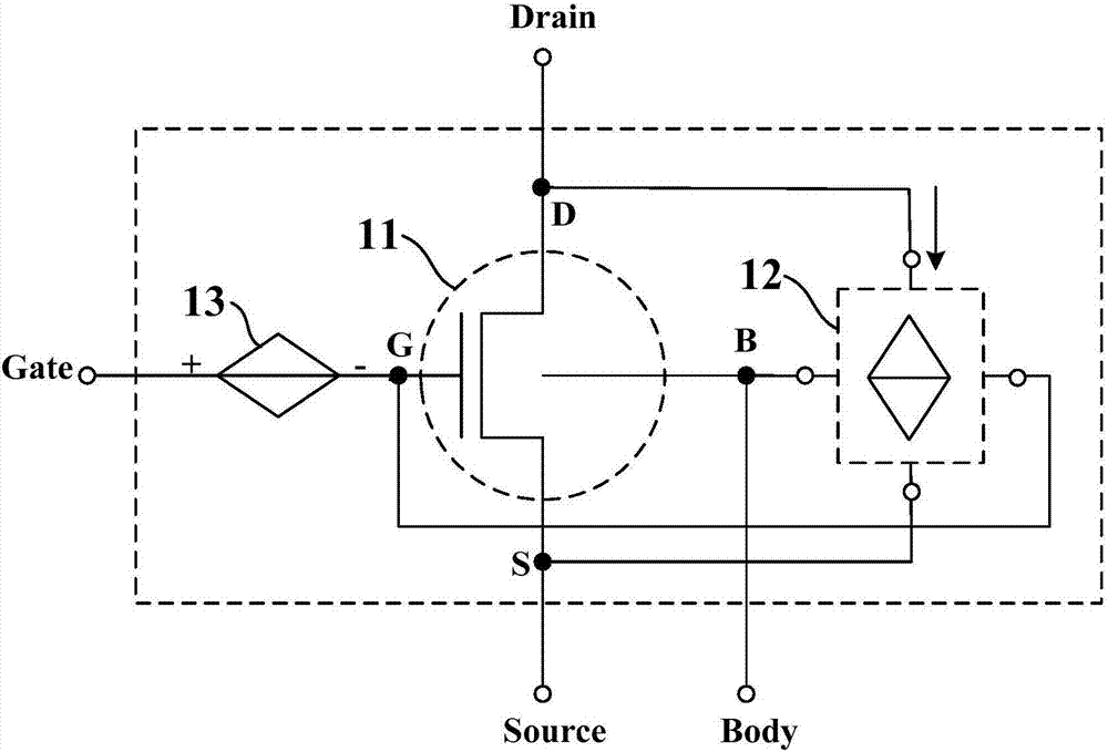
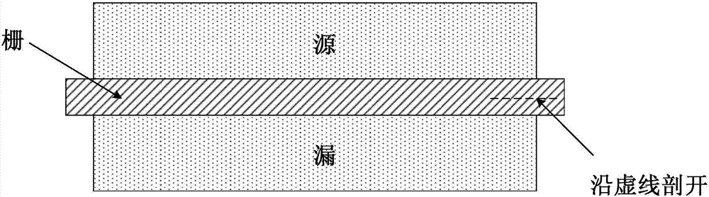
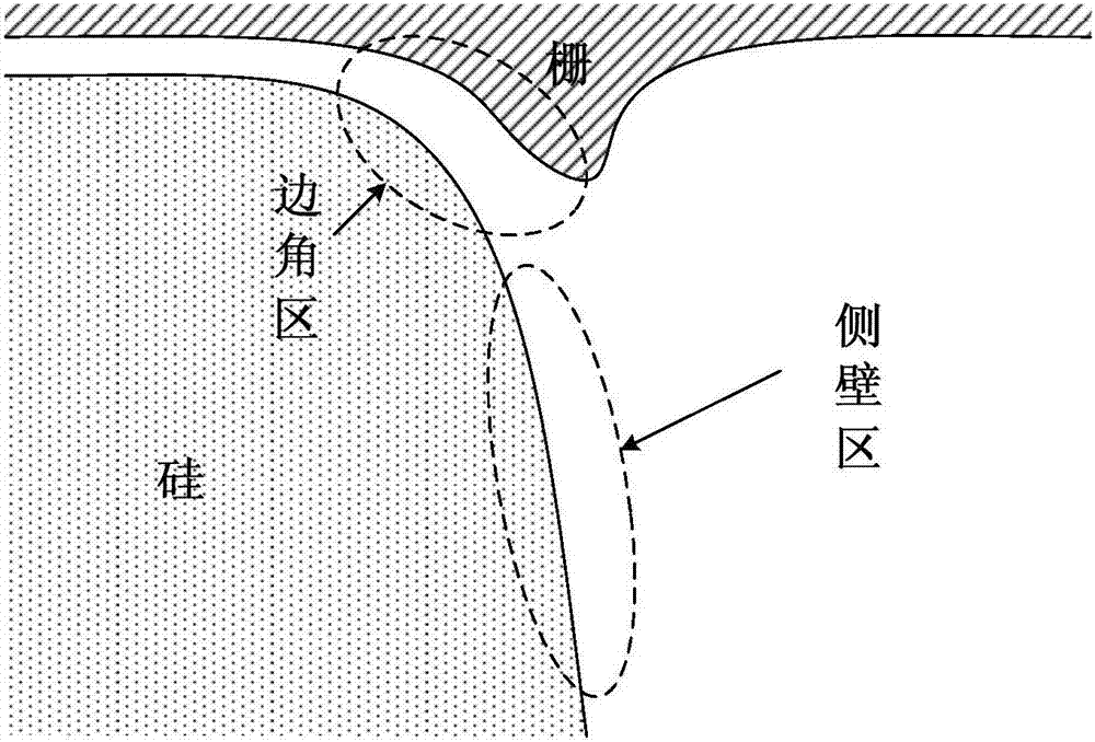
[0038] see Figure 1 to Figure 5 . It should be noted that the diagrams provided in this embodiment are only schematically illustrating the basic idea of ​​the present invention, and only the components related to the present invention are shown in the diagrams rather than the number, shape and shape of the components in actual implementation. Dimensional drawing, the type, quantity and proportion of each component can be changed arb...


PUM


Abstract

The invention provides an SOI MOSFET total dose radiation model building method. The method comprises the steps of establishing a controlled current source, wherein the controlled current source is connected in parallel between the source end and the drain end of an MOSFET device, and the current magnitude of the controlled current source is controlled by the gate end, the source end, the body end and the drain end of the MOSFET device and the total dose; establishing a controlled voltage source, wherein the controlled voltage source is connected in series to the gate end of the MOSFET device, and the voltage size of the controlled voltage source is controlled by the total dose; and packaging the controlled current source, the controlled voltage source and the MOSFET device to form an SOI MOSFET total dose radiation model. According to the SOI MOSFET total dose radiation model building method, an NMOS and a PMOS can be simulated at the same time; the drift of a threshold voltage can be simulated; and the characteristics of MOSFETs with all sizes and all radiation doses can be simulated, so that the simulation accuracy is greatly improved.

Description

technical field [0001] The invention relates to the technical field of device intensive model modeling, in particular to a modeling method of an SOI MOSFET total dose irradiation model. Background technique [0002] SOI (Silicon-On-Insulator, silicon on insulating substrate) is a radiation-resistant silicon-based structure, which can be applied to aerospace electronics and has an inherent immune advantage to cosmic radiation. The total dose effect is an effect that irreversibly affects the device characteristics after a large amount of cosmic rays accumulate in the material, often causing device failure. Although SOI has a special structure, its total dose effect is still obvious, which needs to be alleviated through design and material reinforcement. [0003] The MOSFET intensive model (also called SPICE model) is a model that circuit designers directly invoke to simulate large-scale circuits. It uses specific syntax to express the model, and provides the physical characte...

Claims


Application Information

Patent Timeline
Patent Type & Authority Applications(China)
IPC IPC(8): G06F17/50
CPCG06F30/367
Inventor 陈静黄建强罗杰馨柴展吕凯何伟伟
Owner SHANGHAI INST OF MICROSYSTEM & INFORMATION TECH CHINESE ACAD OF SCI
Why Eureka
Try Eureka