High-voltage device simulation model and modeling method therefor

a high-voltage device and simulation model technology, applied in the field of integrated circuits, can solve the problems of low simulation accuracy, low efficiency and low accuracy and the inability of the simulation model of the high-voltage device to meet the requirements of simulation accuracy, so as to improve the simulation accuracy of the high-voltage device model and high simulation accuracy.

Inactive Publication Date: 2017-01-12
CSMC TECH FAB1
View PDF1 Cites 6 Cited by
  • Summary
  • Abstract
  • Description
  • Claims
  • Application Information

AI Technical Summary

Benefits of technology

[0003]Accordingly, it is necessary to provide a simulation model of a high voltage device and a modeling method thereof, which can have a higher efficiency and simulate characteristics of the high voltage device accurately.
[0006]The above simulation model uses an improved formula among a resistance value and the voltage, the temperature and the width of the high voltage device to correct the resistance value of the voltage-controlled resistor externally coupled to the high voltage device model, which improves the simulation accuracy of the high voltage device model. Even for the ultra high voltage device, such as the ultra high voltage device of which the drain source voltage Vds reaches 700V or more, the high voltage device model can also have a great high simulation accuracy.

Problems solved by technology

This causes that most widely used standard model BSIM3, BSIM4 in the art cannot well fit this kind of high voltage characteristic.
Currently, the simulation model of the high voltage devices has a high cost, a low efficiency and a low accuracy and is time consuming.
Especially for the ultra high voltage devices of which the drain source voltage reaches 700V or more, it is difficult for current simulation model to satisfy the requirement for simulation accuracy.

Method used


Image

  • High-voltage device simulation model and modeling method therefor
  • High-voltage device simulation model and modeling method therefor
  • High-voltage device simulation model and modeling method therefor

Examples


Embodiment Construction

[0011]The above objects, features and advantages of the present invention will become more apparent by describing in detail embodiments thereof with reference to the accompanying drawings. It should be understood that specific embodiments described herein are only used to explain the invention without limiting the invention.

[0012]In the context, “a low voltage”, “a high voltage” and “an ultra high voltage” are distinguished by magnitudes of a gate voltage VGS and a drain source voltage VDS. “a low voltage” refers to 0V≦VGS<5V and 0V≦VDS<5V. “a high voltage” refers to 5V≦VGS≦40V and 5V≦VDS<200V. “an ultra high voltage” refers to VGS≧5V and VDS≧200V, for example VDS is 700V. Further, in the context, “first” and “second” are just used to make a distinction, which does not define any order.

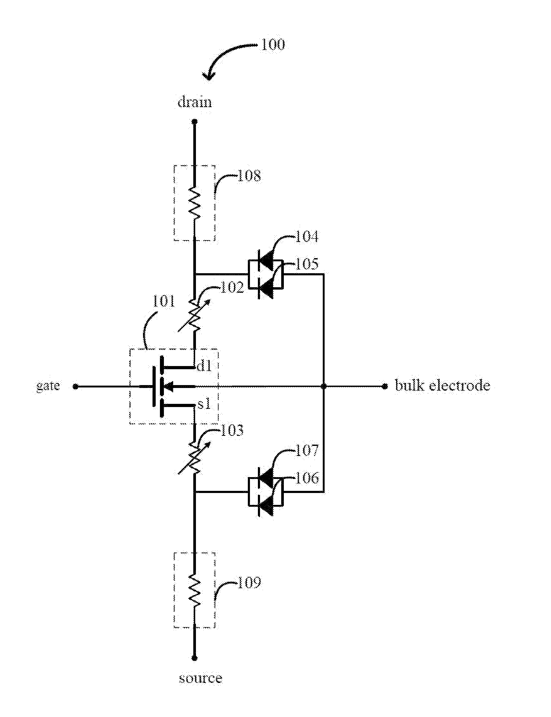
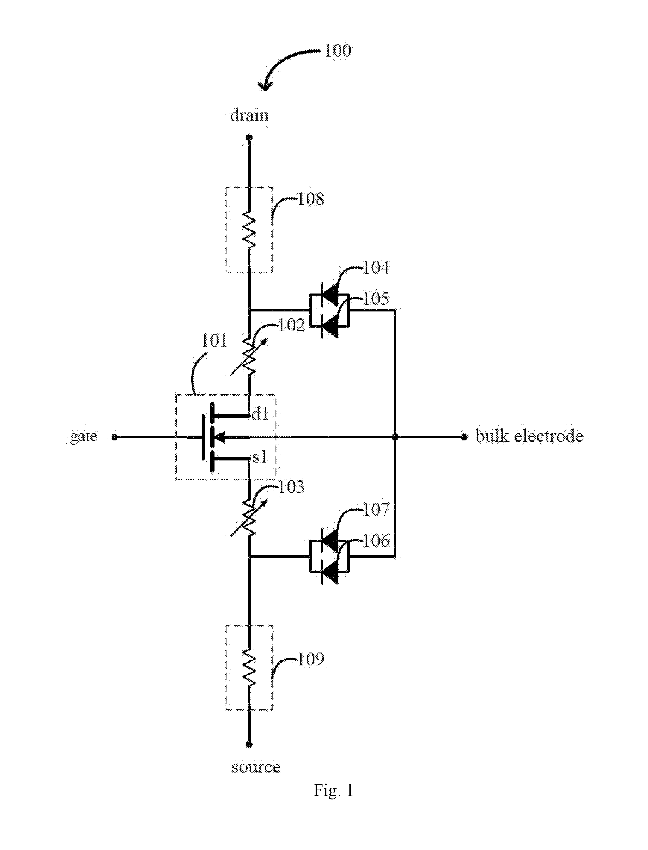
[0013]According to an embodiment of the invention, a simulation model of a high voltage device is provided. FIG. 1 shows a circuit schematic view of a simulation model 100 of a high voltage device in ...


PUM


Abstract

A high-voltage device simulation model and a modeling method thereof are provided. The simulation model comprises: a core transistor (101), a drain terminal resistor (102) and a source terminal resistor (103), wherein a first terminal of the drain terminal resistor (102) is electrically connected to a drain (d1) of the core transistor (101) and a second terminal of the drain terminal resistor (102) serves as the drain of the high voltage device; a first terminal of the source terminal resistor (103) is electrically connected to a source (s1) of the core transistor (101) and a second terminal of the source terminal resistor (103) serves as the source of the high voltage device. The relations of the resistance value of the drain terminal resistor (102) are as follows: RD=(RD0 / W)*(1+CRD*VDERDD+1 / (1+PRWDD*VDERDD))*TFAC_RD, and TFAC_RD=(1+TCRD1*(TEMP−25)+TCRD2*(TEMP−25)*(TEMP−25)).

Description

FIELD OF THE INVENTION[0001]The present invention relates to a field of integrated circuit, and particularly relates to a simulation model of a high voltage device and a modeling method of the simulation model of the high voltage device.BACKGROUND OF THE INVENTION[0002]In recent years, the high voltage devices are widely applied to the integrated circuit products, for example, the high voltage devices can be used in the circuits such as power management chips and the like. With the extensive application of the high voltage devices, in the integrated circuit design, the accuracy required for a simulation model of the high voltage devices is also increased. The special structure of the high voltage devices determines that these devices have greater parasitic effects, such as the typical quasi-saturation effect. The quasi-saturation effect means that when the gate voltage increases, compared with the conventional MOSFET transistor, the increasing speed of saturation current in the high...

Claims


Application Information

Patent Timeline
Patent Type & Authority Applications(United States)
IPC IPC(8): G06F17/50H01L27/02
CPCH01L27/0207G06F17/5009G06F2119/06G06F30/367G06F30/00Y02E60/00Y04S40/20G06F30/20
Inventor HU, YIFENGHE, XIAODONGLIU, XINXIN
Owner CSMC TECH FAB1
Why Eureka
Try Eureka