Manufacturing method of super small unit size vertical super-junction semiconductor device

A technology of superjunction semiconductor and manufacturing method, applied in semiconductor/solid-state device manufacturing, semiconductor devices, electrical components, etc., can solve problems such as limited process limit capability of P-pillar width, inability to further reduce, and process scheme unable to meet requirements, etc.

Active Publication Date: 2017-11-10
WUXI NCE POWER
View PDF6 Cites 5 Cited by
  • Summary
  • Abstract
  • Description
  • Claims
  • Application Information

AI Technical Summary

Problems solved by technology

Moreover, when using the above two methods to manufacture super-junction semiconductor devices, under the condition of the same structural unit size, the width of the P-pillar is limited and the process limit capability cannot be further reduced.
[0006

Method used


Image

  • Manufacturing method of super small unit size vertical super-junction semiconductor device
  • Manufacturing method of super small unit size vertical super-junction semiconductor device
  • Manufacturing method of super small unit size vertical super-junction semiconductor device

Examples


Embodiment Construction

[0031] The present invention will be further described below by taking an N-type trench gate vertical super-junction MOSFET as an example and referring to specific drawings and embodiments. For an N-type super-junction semiconductor device, the first conductivity type is N-type, and the second conductivity type is P-type conductivity; for a P-type super-junction semiconductor device, the first conductivity type is P-type.

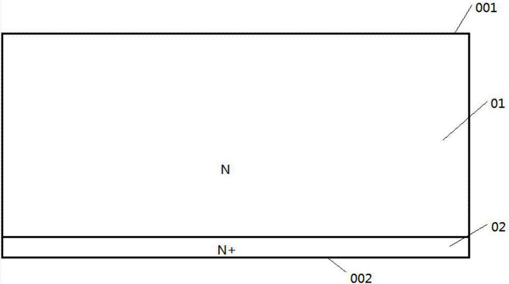
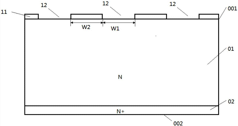
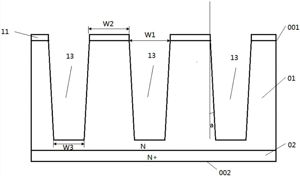
[0032] Such as Figure 8As shown, the ultra-small cell size vertical superjunction semiconductor device includes a semiconductor substrate, and the semiconductor substrate is an N-type semiconductor substrate having a first main surface 001 and a second main surface 002 corresponding to the first main surface 001; The N-type semiconductor substrate is composed of an N-type drift layer 01 including a first main surface 001 and an N+-type substrate 02 including a second main surface 002; the N-type drift layer 01 is provided with a plurality of deep grooves, ...


PUM


Abstract

The invention relates to a manufacturing method of a super small unit size vertical super-junction semiconductor device. The method comprises steps that a hard mask layer is utilized to carry out deep groove etching on a first conductive type semiconductor substrate; a second conductive type epitaxial layer is deposited; anisotropy etching is carried out, and a bottom epitaxial layer of a deep groove is removed; first conductive type impurity injection is carried out; a first conductive type epitaxial layer is deposited to fill the deep groove; planarization of a first main surface of the semiconductor substrate is carried out, the hard mask layer is further removed, the second conductive type epitaxial layer of the side wall of the deep groove forms a second conductive type column of a vertical super-junction structure, and the first conductive type substrate and the first conductive type epitaxial layer respectively form a first conductive type first column and a first conductive type second column. The method is advantaged in that the unit size of the super-junction structure can be substantially reduced on the condition that process difficulty does not increase, and width restrictions of the technology capability in the prior art for the second conductive type column can be broken through.

Description

technical field [0001] The invention relates to a method for manufacturing a super junction semiconductor device, in particular to a method for manufacturing a vertical super junction semiconductor device with an ultra-small unit size. Background technique [0002] In the field of medium and high voltage power semiconductor devices, the vertical super junction structure (Super Junction) has been widely used. Compared with traditional power MOSFET devices, the super junction structure can obtain a better compromise between device withstand voltage and on-resistance. The super junction structure is formed in the drift region of the semiconductor device, extending from the surface of the semiconductor device along the thickness direction to the drift layer body. The super junction structure includes N-conductivity type pillars (N pillars) and P-conductivity type pillars (P pillars), N pillars and A plurality of P-N column pairs formed by alternately adjoining the P columns form...

Claims


Application Information

Patent Timeline
IPC IPC(8): H01L21/336H01L29/06
CPCH01L29/0634H01L29/66666
Inventor 朱袁正李宗清
Owner WUXI NCE POWER
Why Eureka
Try Eureka