Supercharge Your Innovation With Domain-Expert AI Agents!

Display panel and manufacturing method thereof

A technology for a display panel and a manufacturing method, which is applied to the manufacture of semiconductor/solid-state devices, electrical components, and electrical solid-state devices, etc., can solve problems such as affecting display effects, uneven display of self-luminous panels, and color mixing, and achieves improved luminous efficiency, optimized Panel process and yield, the effect of reducing color shift

Inactive Publication Date: 2017-11-17
HKC CORP LTD +1
View PDF2 Cites 9 Cited by
  • Summary
  • Abstract
  • Description
  • Claims
  • Application Information

AI Technical Summary

Problems solved by technology

This traditional process has a large number of channels and the process is complex, but if the pixel definition layer is omitted, it will cause uneven display or color mixing of the self-luminous panel, which will affect the display effect

Method used


Image

  • Display panel and manufacturing method thereof
  • Display panel and manufacturing method thereof
  • Display panel and manufacturing method thereof

Examples


Embodiment Construction

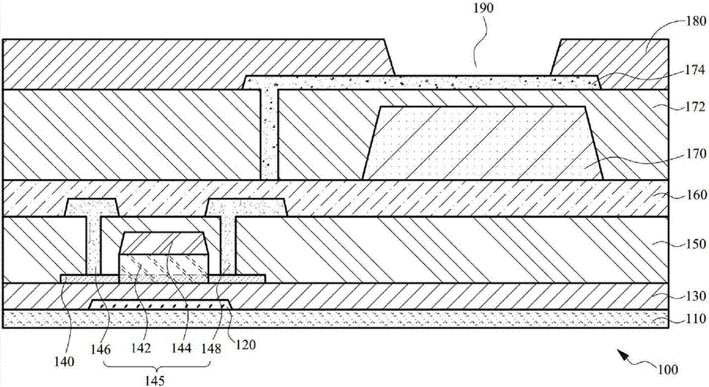
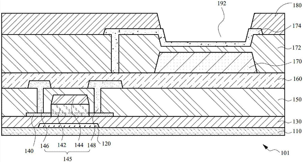
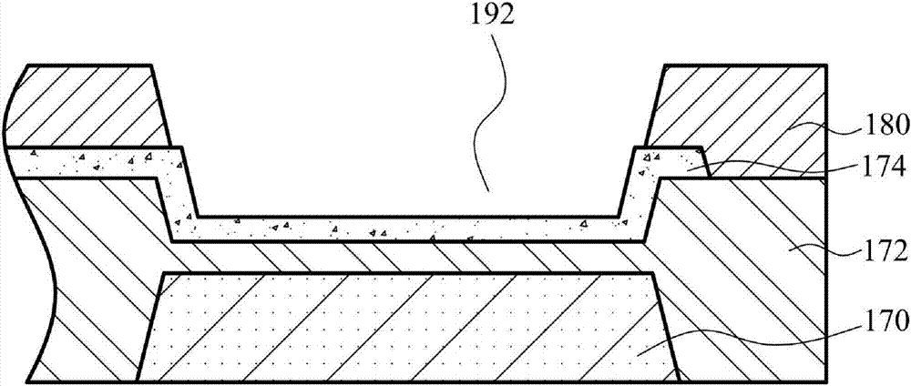
[0023] The following descriptions of the various embodiments refer to the attached drawings to illustrate specific embodiments that the present application can be implemented in. The directional terms mentioned in this application, such as "up", "down", "front", "rear", "left", "right", "inside", "outside", "side", etc., are for reference only The orientation of the attached schema. Therefore, the directional terms used are used to illustrate and understand the application, but not to limit the application.

[0024] The drawings and descriptions are to be regarded as illustrative in nature and not restrictive. In the figures, structurally similar units are denoted by the same reference numerals. In addition, the size and thickness of each component shown in the drawings are arbitrarily shown for understanding and convenience of description, but the present application is not limited thereto.

[0025] In the drawings, the thickness of layers, films, panels, regions, etc., ar...


PUM


Abstract

The present invention provides a display panel and a manufacturing method thereof. The display panel includes a substrate, a plurality of active switches, a passivation layer, a pixel definition layer, a planarization layer, a color resistance layer and a transparent electrode layer; the plurality of active switches are disposed on the substrate; the passivation layer is disposed on the substrate and covers the active switches; the pixel definition layer is disposed on the passivation layer and is provided with a plurality of light-emitting elements; the planarization layer is disposed between the passivation layer and the pixel definition layer; a groove structure is formed in the planarization layer; the color resistance layer is disposed between the passivation layer and the planarization layer and is aligned with the groove structure of the planarization layer; and the transparent electrode layer is disposed on the planarization layer and covers the groove structure; and the light-emitting elements are disposed in the groove structure of the planarization layer and are aligned with the color resistance layer. With the manufacturing method thereof of the present invention adopted, the light-emitting efficiency of a self-luminous panel can be improved, the manufacturing process and yield of the panel can be optimized, and the color cast phenomena of the self-luminous display panel can be decreased.

Description

technical field [0001] The present application relates to a display panel and a manufacturing method thereof, in particular to a light emitting diode display panel and a manufacturing method thereof. Background technique [0002] At present, high-pixel flat display panels are the market trend, and AMOLED (Active Matrix / Organic Light Emitting Diode, active matrix organic light-emitting diode) panels have attracted everyone's attention, and AMOLED panels are in the small and medium-sized panel market with 200ppi pixels. Occupying a dominant position, AMOLED WVGA (Wide Video Graphics Array, a resolution higher than VGA resolution: 800*480; ~200ppi) is the current mainstream resolution, while high-pixel 250ppi, 300ppi and 350ppi will be the future development trend. The existing AMOLED panel production method is mainly based on Side by Side (side by side) technology, but the technology has certain difficulties in producing products with 300ppi and above. Therefore, the industr...

Claims


Application Information

Patent Timeline
IPC IPC(8): H01L27/32H01L51/56
CPCH10K59/124
Inventor 卓恩宗田轶群杨凤云樊堃
Owner HKC CORP LTD
Features
  • R&D
  • Intellectual Property
  • Life Sciences
  • Materials
  • Tech Scout
  • Unparalleled Data Quality
  • Higher Quality Content
  • 60% Fewer Hallucinations
Learn More