
Pixel reading circuit, array reading circuit and pixel reading method

A technology for reading circuits and pixels, applied in the field of photoelectric detection, can solve the problems of complex design and high cost of the analog front-end of the reading circuit, and achieve the effect of reducing the number, simplifying the design, and reducing the cost.

Inactive Publication Date: 2017-11-24
BOE TECH GRP CO LTD
View PDF5 Cites 0 Cited by
  • Summary
  • Abstract
  • Description
  • Claims
  • Application Information

AI Technical Summary

Problems solved by technology

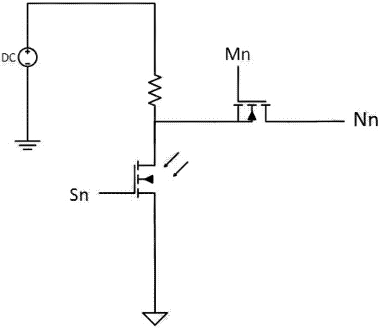
[0003] The currently widely used pixel reading circuit includes a photosensitive transistor and a transistor, such as figure 1 As shown, the gate of the phototransistor is connected to the scanning signal terminal Sn, the source is connected to the ground potential, the drain is connected to the source of the transistor, the source of the transistor is also connected to a DC power supply voltage DC through a resistor, and the gate of the transistor is connected to the enable signal Terminal Mn, the drain of the transistor is the signal output terminal Nn; when the pixel reading circuit with this structure is used for array image reading, the scanning signal of each pixel row must be controlled separately to avoid mutual interference between pixel rows, which The analog front-end design of the read circuit is complicated and expensive

Method used


Image

  • Pixel reading circuit, array reading circuit and pixel reading method
  • Pixel reading circuit, array reading circuit and pixel reading method
  • Pixel reading circuit, array reading circuit and pixel reading method

Examples


Embodiment 1

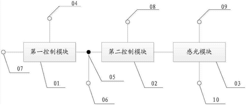
[0048] refer to figure 2 , shows a schematic structural diagram of a pixel reading circuit provided in the first embodiment, and the pixel reading circuit includes: a first control module 01 , a second control module 02 and a photosensitive module 03 .

[0049] The first control module 01 is respectively connected to the first enable signal input terminal 04, the first node 05 and the voltage signal output terminal 07, the first node 05 is connected to the first voltage signal input terminal 06, and the first control module 01 is used to The enable signal and the voltage of the first node 04 output a voltage signal to the voltage signal output terminal 07 .

[0050] The second control module 02 is respectively connected to the second enabling signal input terminal 08, the photosensitive module 03 and the first node 05, and is used to control the on and off between the photosensitive module 03 and the first control module 01 according to the second enabling signal open.

[0...

Embodiment 2

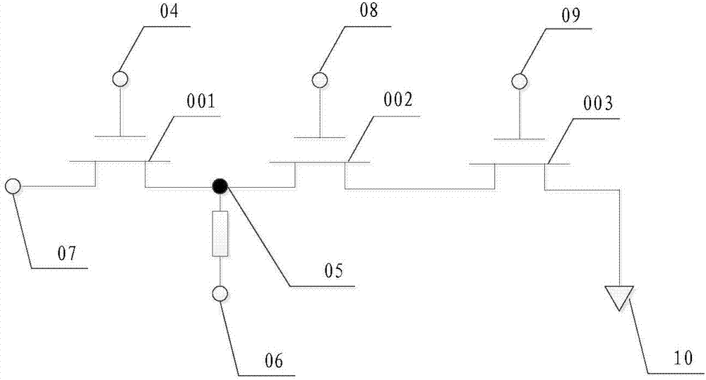
[0062] refer to image 3 , shows a schematic structural diagram of a pixel reading circuit provided in Embodiment 2, where the pixel reading circuit includes a first transistor 001 , a second transistor 002 and a photosensitive transistor 003 .

[0063] The first transistor 001 includes a first control electrode, a first electrode and a second electrode; the first control electrode is connected to the first enable signal input terminal 04, the first electrode is connected to the first node 05, and the first node 05 is connected to the first The voltage signal input terminal 06 , and the second electrode is connected to the voltage signal output terminal 07 .

[0064] The second transistor 002 includes a second control electrode, a third electrode and a fourth electrode; the second control electrode is connected to the second enable signal input terminal 08 , the third electrode is connected to the phototransistor 003 , and the fourth electrode is connected to the first node 05...

Embodiment 3

[0075] refer to Figure 4 , which shows a schematic structural diagram of an array readout circuit provided in the third embodiment, the array readout circuit includes a plurality of pixel readout circuits as in any of the above-mentioned embodiments, and the plurality of pixel readout circuits are arranged in an array .

[0076] The scanning signal input terminals of the pixel reading circuits in each row are connected to the total scanning signal input terminal S.

[0077] The first voltage signals input to the first voltage signal input terminals of the pixel reading circuits in each row are the same.

[0078] The second voltage signals input by the second voltage signal input terminals of the pixel reading circuits in each row are the same.

[0079] The first enable signal input end and the second enable signal input end of each row of the pixel reading circuit are connected to the row enable signal input ends M1, M2 . . . Mn.

[0080] The voltage signal output terminal...


PUM


Abstract

The invention provides pixel reading circuits, an array reading circuit and a pixel reading method; the pixel reading circuit comprises a first control module, a second control module and photographic modules; the photographic module outputs a voltage signal to the second control module according to a scanning signal and a first threshold-voltage changing with photographic quantities; the second control module controls the photographic module to connect with / disconnect from the first control module according to a second enabling signal; the first control module outputs a photographic signal according to a first enabling signal. The pixel reading circuit can use the first and second enabling signals to select a working line and a non-working line in an array image reading process; the second control module is arranged so as to prevent a working line outputted photographic signal from being pulled up or down when a non-working line photographic module is open; all pixel reading circuits can share one simulation scanning signal, thus reducing simulation signal source quantity, simplifying the simulation front end designs, and reducing cost.

Description

technical field [0001] The invention relates to the technical field of photodetection, in particular to a pixel reading circuit, an array reading circuit and a pixel reading method. Background technique [0002] The technology of obtaining corresponding images according to the distribution of light intensity is applied to many devices. For example, infrared imagers use photoelectric detection technology to detect infrared band signals of thermal radiation of objects, and convert the signals into images and graphics that can be visually distinguished by humans. And can further calculate the temperature distribution of the object. Infrared imaging technology enables human beings to transcend visual barriers, so that people can see the temperature distribution on the surface of objects. Among them, the process of converting the acquired light signal into an image needs to be completed by the pixel reading circuit. [0003] The currently widely used pixel reading circuit inclu...

Claims


Application Information

Patent Timeline
Patent Type & Authority Applications(China)
IPC IPC(8): G01J5/10G01J5/02
CPCG01J5/02G01J5/10
Inventor 史永明王纯
Owner BOE TECH GRP CO LTD
Learn More