Supercharge Your Innovation With Domain-Expert AI Agents!

Display device

A display device and conductive layer technology, applied in nonlinear optics, instruments, optics, etc., can solve problems such as complex improvement process, difficult implementation, etc., and achieve the effect of improving anti-interference ability and weakening interference

Active Publication Date: 2017-11-24
KUSN INFOVISION OPTOELECTRONICS
View PDF16 Cites 1 Cited by
  • Summary
  • Abstract
  • Description
  • Claims
  • Application Information

AI Technical Summary

Problems solved by technology

[0003] However, since the GIA circuit contains multiple thin film transistors, the interference of the external electric field will affect the display effect of the entire liquid crystal display device. The interference is also relatively large
[0004] The prior art usually solves the above-mentioned technical problems by improving manufacturing capacity or improving materials, but due to the complexity and difficulty of this improvement process, it is difficult to implement

Method used


Image

  • Display device
  • Display device
  • Display device

Examples


Embodiment Construction

[0022] Hereinafter, the present invention will be described in more detail with reference to the accompanying drawings. In the various figures, identical elements are indicated with similar reference numerals. For the sake of clarity, various parts in the drawings have not been drawn to scale. Also, some well-known parts may not be shown in the drawings.

[0023] In the following, many specific details of the present invention are described, such as device structures, materials, dimensions, processing techniques and techniques, for a clearer understanding of the present invention. However, the invention may be practiced without these specific details, as will be understood by those skilled in the art.

[0024] Hereinafter, the present invention will be described in detail with reference to the accompanying drawings.

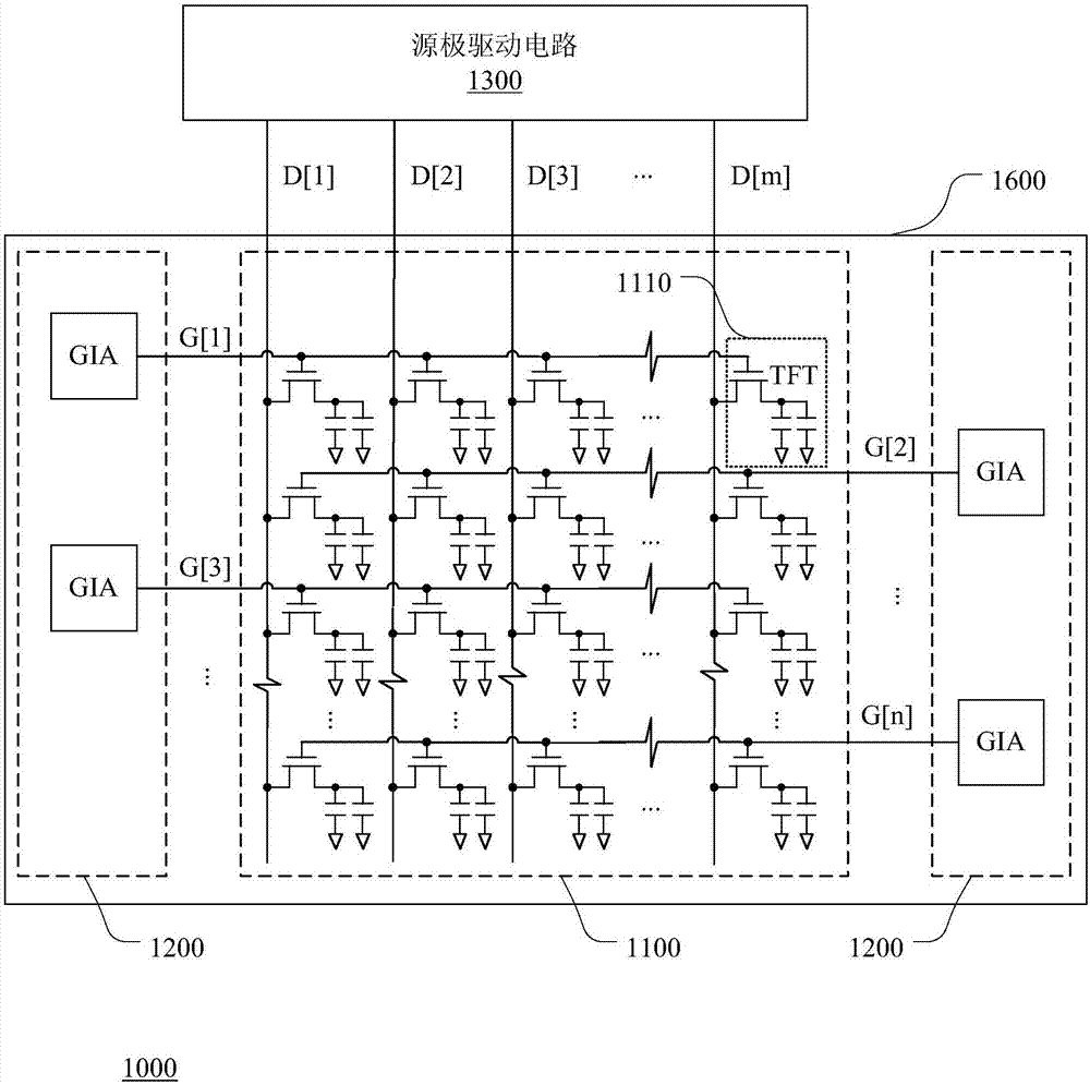
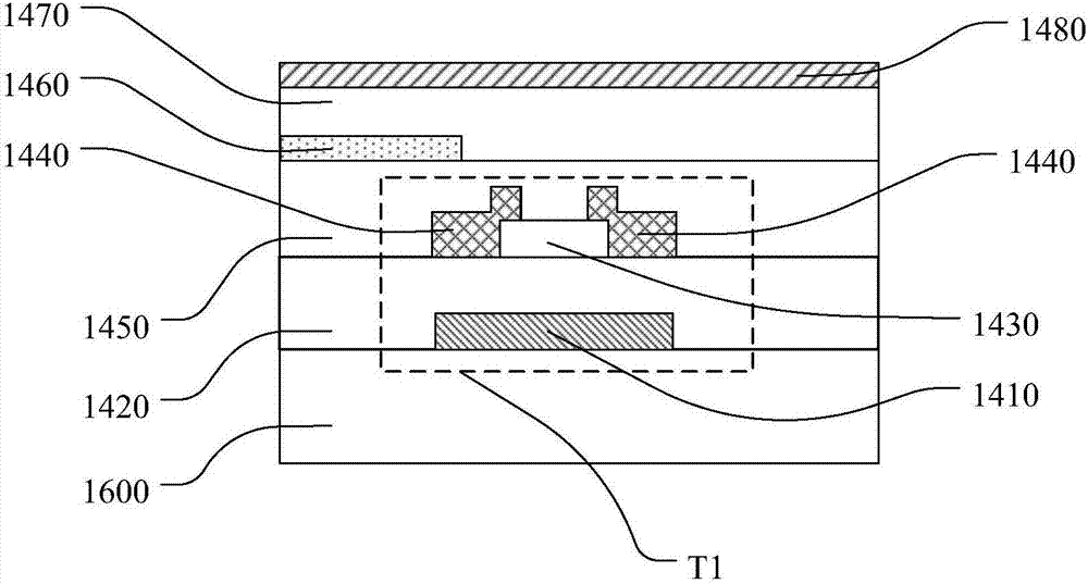
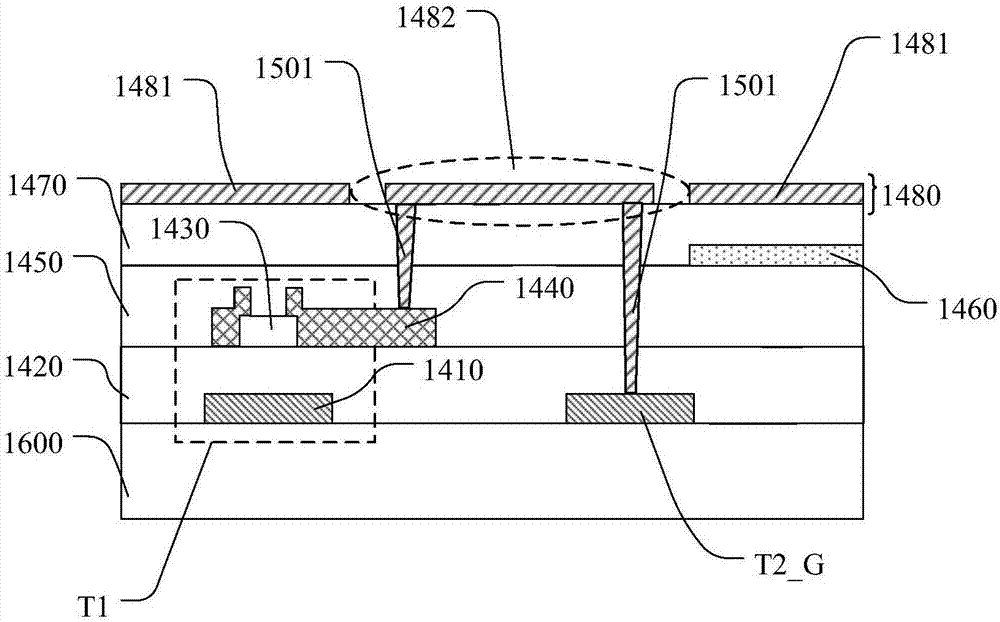
[0025] figure 1 A schematic structural diagram of a display device according to a first embodiment of the present invention is shown.

[0026] like figure ...


PUM


Abstract

The invention discloses a display device. The device comprises a substrate, multiple transistors and a first conducting layer. The first surface of the substrate comprises a first section used for formation of a pixel array and a second section used for formation of gate driving circuits; the multiple transistors are formed in the second section of the substrate and used for constituting at least one part of the gate driving circuits; the first conducting layer is arranged above the multiple transistors and isolated from the multiple transistors, the first conducting layer comprises a conductor structure corresponding to the second section of the substrate, and the conductor structure is grounded or receives a set voltage. According to the device, through arrangement of the conductor structure which is grounded or receives the set voltage, shielding of GIA circuits in the display device is achieved, and due to no change of process, the anti-interference capability of the GIA circuits is improved on the basis of no increase of the cost while interference with other circuits such as a touch device by the GIA circuits is reduced, so that the display effect of the display device is guaranteed, and the performance of the whole display device and other devices connected with the display device is improved.

Description

technical field [0001] The present invention relates to the field of display technology, and more specifically, to a display device. Background technique [0002] With the development of the liquid crystal display (Liquid Crystal Display, LCD) industry, the visual effect of narrow borders has become a mainstream trend of high-quality display screens. In order to further reduce the frame width of the liquid crystal display device, the most common practice in the industry is to manufacture the gate driver circuit on the array substrate of the liquid crystal display device to form an integrated gate driver (Gate Driver In Array, GIA) circuit, so that both It does not need to be connected with an additional gate driver chip, and the frame of the liquid crystal display device can be made very narrow. [0003] However, since the GIA circuit contains multiple thin film transistors, the interference of the external electric field will affect the display effect of the entire liquid ...

Claims


Application Information

Patent Timeline
IPC IPC(8): G02F1/1345G02F1/1333
CPCG02F1/13338G02F1/13452G02F1/13454G02F2202/22
Inventor 黄清英蒋隽
Owner KUSN INFOVISION OPTOELECTRONICS
Features
  • R&D
  • Intellectual Property
  • Life Sciences
  • Materials
  • Tech Scout
  • Unparalleled Data Quality
  • Higher Quality Content
  • 60% Fewer Hallucinations
Learn More