Thin-film transistor array, image display device, and method for manufacturing thin-film transistor array
A technology of thin-film transistors and arrays, which is applied in the manufacturing fields of thin-film transistor arrays, image display devices, and thin-film transistor arrays. It can solve the problems of low patterning yield, short circuit of gate wiring and capacitor wiring, etc., to prevent damage and realize low-temperature process Effect
- Summary
- Abstract
- Description
- Claims
- Application Information
AI Technical Summary
Problems solved by technology
Method used
Image

Examples
no. 1 approach
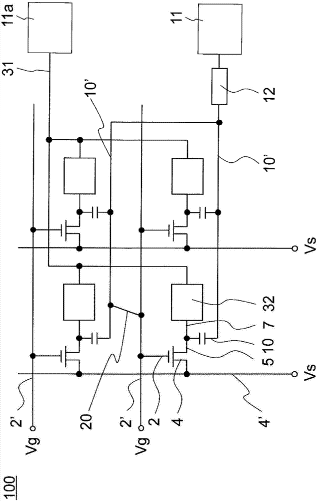
[0054] figure 1 The thin film transistor array 100 according to the first embodiment is shown in . The thin film transistor array 100 has: an insulating substrate 1; a plurality of gate electrodes 2 formed on the insulating substrate 1, a plurality of gate wirings 2' connected to the gate electrodes 2, a plurality of capacitor electrodes 10, and A plurality of capacitor wirings 10'; a gate insulating film 3 formed on the insulating substrate 1, a gate electrode 2, a gate wiring 2', a capacitor electrode 10, and a capacitor wiring 10'; a plurality of capacitors formed on the gate insulating film 3 A source electrode 4, a plurality of source wiring 4' connected to the source electrode 4, a plurality of drain electrodes 5, and a plurality of pixel electrodes 7 connected to the drain electrode 5, the pixel electrode 7 and the capacitor electrode via the gate insulating film 3 10 overlapping to have a storage capacitor, the source electrode 4 and the drain electrode 5 overlap the ...
no. 2 approach
[0070] Figure 4 A thin film transistor array 200 according to the second embodiment is shown in . The thin film transistor array 200 has: an insulating substrate 1; a plurality of gate electrodes 2 formed on the insulating substrate 1, a plurality of gate wirings 2' connected to the gate electrodes 2, a plurality of capacitor electrodes 10, and A plurality of capacitor wirings 10'; a gate insulating film 3 formed on the insulating substrate 1, a gate electrode 2, a gate wiring 2', a capacitor electrode 10, and a capacitor wiring 10'; a plurality of capacitors formed on the gate insulating film 3 A source electrode 4, a plurality of source wiring 4' connected to the source electrode 4, a plurality of drain electrodes 5, and a plurality of pixel electrodes 7 connected to the drain electrode 5, the pixel electrode 7 and the capacitor electrode via the gate insulating film 3 10 overlapping to have a storage capacitor, the source electrode 4 and the drain electrode 5 overlap the ...
Embodiment 1
[0097] Specific examples will be described. As Example 1, using Figure 3A ~ Figure 3G The process shown produces Figure 2A The thin film transistor array 100 is shown. First, a glass substrate was prepared as an insulating substrate 1, Ag ink was offset-printed and sintered to form a gate electrode 2, a gate wiring 2', a capacitor electrode 10, and a capacitor wiring 10' ( Figure 3A ).
[0098] Next, the polyvinylphenol solution was die coated and fired to form the gate insulating film 3 ( Figure 3B ).
[0099] Then, Ag ink is carried out offset printing and sintering, has formed source electrode 4, source electrode wiring 4 ', drain electrode 5 and pixel electrode 7 ( Figure 3C ). Next, the polythiophene organic semiconductor solution was flexographically printed and sintered to form a semiconductor layer 6 ( Figure 3D ). Then, the fluororesin solution is screen-printed and sintered to form a protective layer 6' ( Figure 3E ).
[0100] Next, a 10 kΩ chip resi...
PUM
| Property | Measurement | Unit |
|---|---|---|
| contact resistance | aaaaa | aaaaa |
Abstract
Description
Claims
Application Information
 - R&D
- Intellectual Property
- Life Sciences
- Materials
- Tech Scout
- Unparalleled Data Quality
- Higher Quality Content
- 60% Fewer Hallucinations
Browse by: Latest US Patents, China's latest patents, Technical Efficacy Thesaurus, Application Domain, Technology Topic, Popular Technical Reports.
© 2025 PatSnap. All rights reserved.Legal|Privacy policy|Modern Slavery Act Transparency Statement|Sitemap|About US| Contact US: help@patsnap.com