A pixel compensation method, pixel compensation device and display device

A technology of compensation method and compensation device, which is applied to static indicators, instruments, etc., can solve problems such as inaccurate data voltage, inaccurate voltage, and affecting the display effect of the screen

Active Publication Date: 2019-07-09
BOE TECH GRP CO LTD
View PDF5 Cites 0 Cited by
  • Summary
  • Abstract
  • Description
  • Claims
  • Application Information

AI Technical Summary

Problems solved by technology

Due to the effect of the coupling capacitor, the signal of the detection line will change when the electroluminescent display panel switches screens, resulting in inaccurate detected voltage on the detection line, which in turn leads to inaccurate data voltage obtained through compensation calculation, which affects the display of the screen problem of effect

Method used


Image

  • A pixel compensation method, pixel compensation device and display device
  • A pixel compensation method, pixel compensation device and display device
  • A pixel compensation method, pixel compensation device and display device

Examples


Embodiment 1

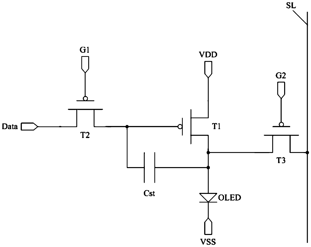
[0060] During specific implementation, in the pixel compensation method provided by the embodiment of the present invention, each color sub-pixel to be compensated in row 2n-1 inputs a data voltage corresponding to a non-zero gray scale, and each color sub-pixel to be compensated in row 2n inputs The data voltage corresponding to the zero gray scale; and sequentially charging the detection lines corresponding to the color sub-pixels to be compensated in the 2n-1th row and the 2nth row, which may specifically include: sequentially controlling each of the 2n-1th row and the 2nth row The pixel circuit in the sub-pixel of the color to be compensated operates and charges the connected detection line. Among them, since the non-zero gray scale corresponds to the rest of the picture except the blackest picture, the driving transistor in the pixel circuit can generate an operating current, so the data voltage corresponding to the non-zero gray scale is charged to the connected detection...

Embodiment 2

[0068] During specific implementation, in the pixel compensation method provided by the embodiment of the present invention, each sub-pixel of the color to be compensated in the 2n-1th row inputs the data voltage corresponding to the zero gray scale, and each sub-pixel of the color to be compensated in the 2nth row inputs the non- The data voltage corresponding to the zero gray scale; and, sequentially charging the detection lines corresponding to the color sub-pixels to be compensated in the 2n-1th row and the 2nth row, specifically including: sequentially controlling each of the 2n-1th row and the 2nth row The pixel circuit in the sub-pixel of the color to be compensated operates and charges the connected detection line. Among them, since the non-zero gray scale corresponds to the rest of the picture except the blackest picture, the driving transistor in the pixel circuit can generate an operating current, so the data voltage corresponding to the non-zero gray scale is charge...


PUM


Abstract

The invention discloses a pixel compensation method, a pixel compensation device and a display device. In the blanking area of ​​two adjacent display frames, the sub-pixels corresponding to the color sub-pixels to be compensated in the 2n-1 row and the 2n row are sequentially The detection line is charged, one line corresponds to the input of non-zero gray scale, and the other line corresponds to the input of zero gray scale; respectively detect the voltage on the detection line corresponding to each sub-pixel of the color to be compensated in the line corresponding to the input non-zero gray scale and zero gray scale; according to The voltage corresponding to the color sub-pixel to be compensated in the 2n-1 row and the 2n-th row and belonging to the same column can obtain the detection voltage corresponding to each color sub-pixel to be compensated in the row corresponding to the input non-zero gray scale, so as to eliminate the coupling effect on the detection The influence of the voltage can improve the accuracy of each detected voltage, improve the problem of inaccurate data voltage obtained by compensation and calculation due to the voltage change on the detection line caused by the coupling effect, and improve the display effect of the screen.

Description

technical field [0001] The invention relates to the field of display technology, in particular to a pixel compensation method, a pixel compensation device and a display device. Background technique [0002] Electroluminescent diodes (Organic Light Emitting Diode, OLED), Quantum Dot Light Emitting Diodes (Quantum Dot Light Emitting Diodes, QLED) and other electroluminescent diodes have the advantages of self-luminescence, low energy consumption, etc. One of the hot spots. Currently, electroluminescent diodes are generally current-driven, requiring a stable current to drive them to emit light. In addition, pixel circuits are used in the electroluminescent display panel to drive the electroluminescent diodes to emit light. Existing pixel circuits such as figure 1 As shown, it generally includes: a driving transistor T1, a switching transistor T2 and a storage capacitor Cst. The pixel circuit controls the switching transistor T2 to open to write the data voltage of the data ...

Claims


Application Information

Patent Timeline
Patent Type & Authority Patents(China)
IPC IPC(8): G09G3/3208
CPCG09G3/3208G09G3/3233G09G2320/0209G09G2320/045G09G2320/0295G09G2320/0233G09G3/3258
Inventor 李永谦冯雪欢
Owner BOE TECH GRP CO LTD
Why Eureka
Try Eureka