Pixel circuit and driving method thereof, display substrate and driving method thereof, and display apparatus

A pixel circuit and display substrate technology, applied in the field of pixel circuit and its driving method, display device, display substrate and its driving, can solve the problems of short-term afterimage, brightness difference, etc.

Active Publication Date: 2017-12-08
BOE TECH GRP CO LTD
View PDF6 Cites 39 Cited by
  • Summary
  • Abstract
  • Description
  • Claims
  • Application Information

AI Technical Summary

Problems solved by technology

It can be seen from this that due to the different paths of voltage changes during the charge trapping and releasing processes, the drive currents Ids corresponding to points A2 and A4 that reach the voltage V_g along different paths are different, so that the co

Method used


Image

  • Pixel circuit and driving method thereof, display substrate and driving method thereof, and display apparatus
  • Pixel circuit and driving method thereof, display substrate and driving method thereof, and display apparatus
  • Pixel circuit and driving method thereof, display substrate and driving method thereof, and display apparatus

Examples


Example Embodiment

[0034] The technical solutions in the embodiments of the present invention will be clearly and completely described below with reference to the accompanying drawings in the embodiments of the present invention. Obviously, the described embodiments are only a part of the embodiments of the present invention, but not all of the embodiments. Based on the embodiments of the present invention, all other embodiments obtained by those of ordinary skill in the art without creative efforts shall fall within the protection scope of the present invention.
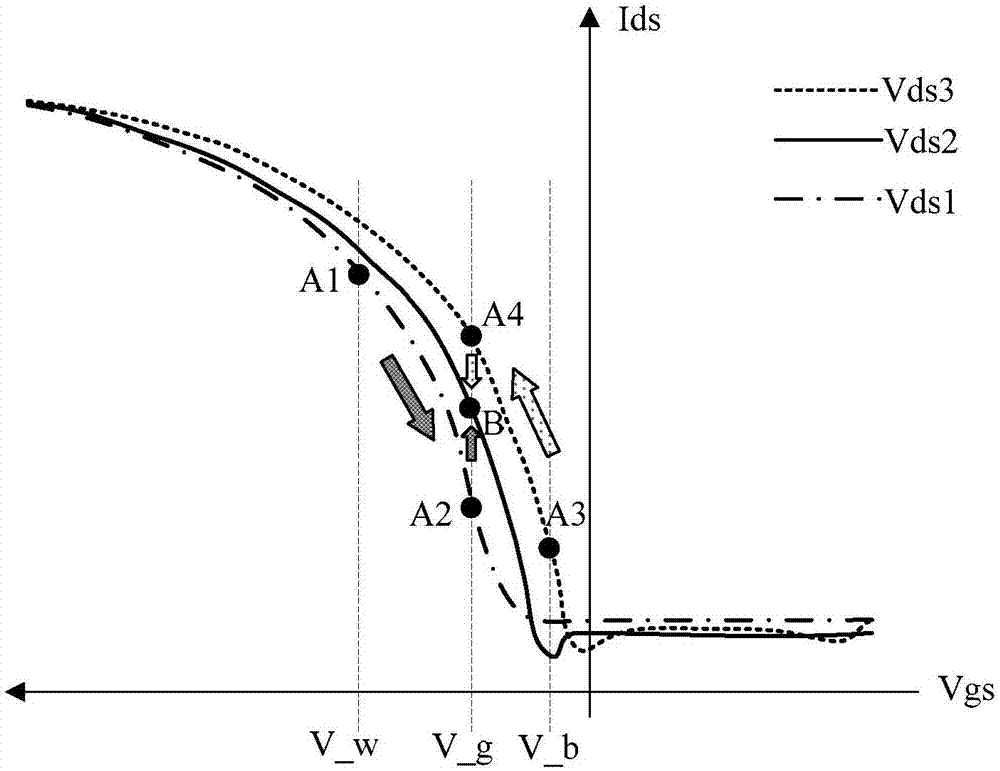
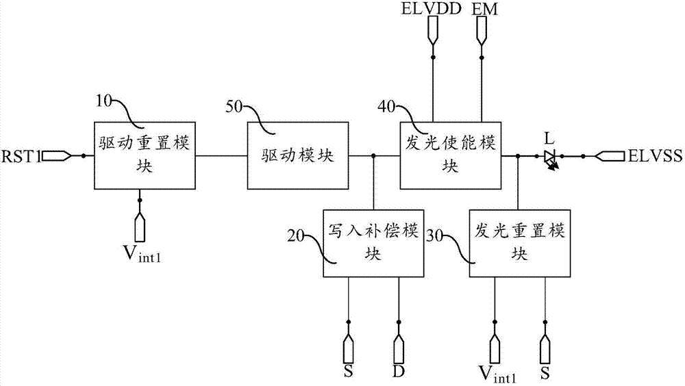
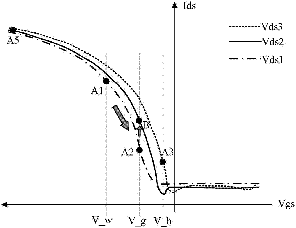
[0035] Embodiments of the present invention provide a pixel circuit, such as figure 2 As shown, it includes: a driving reset module 10, a writing compensation module 20, a light-emitting reset module 30, a light-emitting enabling module 40, a driving module 50 and a light-emitting device L; the driving module 50 includes a driving transistor Td (such as Figure 4 shown), the first pole of the driving transistor Td is connected to the...


PUM


Abstract

An embodiment of the invention provides a pixel circuit and a driving method thereof, a display substrate and a driving method thereof, and a display apparatus and relates to the display technology field. In the embodiment of the invention, short-term residual image problem can be improved. The pixel circuit comprises a driving reset module, a writing-in compensation module, a luminescence reset module and a luminescence enablement module, wherein the driving reset module inputs a voltage of a first initial voltage terminal to a grid electrode of a driving transistor in a driving module under control of a first reset signal terminal; the writing-in compensation module is used for inputting a reference voltage output by a data voltage terminal in a shadow elimination phase to the driving module under control of a scanning signal terminal so that the driving transistor is in a conduction state; in a writing-in compensation phase, the data voltage is input to the driving module and the driving module is compensated; the luminescence reset module is used for inputting the voltage of the first initial voltage terminal to a luminescent device so as to carry out reset under the control of the scanning signal terminal; and the luminescence enablement module is used for providing a voltage of a first power supply voltage terminal for the driving module under the control of an enablement signal terminal and making the driving module be connected to the luminescent device.

Description

technical field [0001] The present invention relates to the field of display technology, in particular to a pixel circuit and a driving method thereof, a display substrate and a driving method thereof, and a display device. Background technique [0002] Organic Light Emitting Diode (OLED) display is one of the hotspots in the current research field. Compared with Liquid Crystal Display (LCD), OLED has low energy consumption, low production cost, self-illumination, and wide viewing angle. And corresponding advantages such as fast speed. [0003] Analysis shows that the above-mentioned short-term afterimage phenomenon is related to the hysteresis effect of the driving transistor in the OLED display. The process of the hysteresis effect is as figure 1 As shown, among them, figure 1 The middle dotted line is the characteristic curve of the current Ids of the driving transistor and the gate-source voltage (Vgs) when the source-drain voltage of the driving transistor in the sub...

Claims


Application Information

Patent Timeline
IPC IPC(8): G09G3/3208
CPCG09G3/3208G09G2320/0257G09G3/3233G09G2300/0819G09G2300/0861G09G2300/0842G09G2320/043G09G2310/0251G09G3/3258G09G2300/0426
Inventor 高雪岭羊振中彭宽军秦纬邹祥祥杨洋
Owner BOE TECH GRP CO LTD
Why Eureka
Try Eureka