Array substrate and manufacturing method thereof and liquid crystal panel

An array substrate and manufacturing method technology, applied in the field of display, can solve the problems of lowered transmittance, low etching rate of color-resist patterns, unable to precipitate gas, etc., and achieve the effect of reducing risks

Inactive Publication Date: 2017-12-12
TCL CHINA STAR OPTOELECTRONICS TECH CO LTD
View PDF5 Cites 17 Cited by
  • Summary
  • Abstract
  • Description
  • Claims
  • Application Information

AI Technical Summary

Problems solved by technology

[0002] The liquid crystal panel based on COA (Color Filter on Array, color filter array) technology is prone to produce bubbles (bubbles) when it hits. The vias of transistors overlap, and the PV layer (Passivation, passivation layer) at the overlapping position is etched away, causing the gas in the color resistance pattern to precipitate from the overlapping position after the box forming process and form Bubbles. The improvement countermeasure is to expand the color resistance The size of the via hole of the pattern so that it does not overlap with the TFT via hole, but this will reduce the penetration rate
The second is that during the vibration process, due to the cracking of the PV layer, the gas in the color resistance pattern is precipitated to form bubbles. The improvement countermeasure is to open a small-sized vent hole on the color resistance pattern, and the gas in the color resistance pattern passes through the vent hole. It is discharged before the box forming process, but the etching rate of the color resist pattern is lower than that of the PV layer, and the gas cannot be precipitated due to insufficient etching depth.

Method used


Image

  • Array substrate and manufacturing method thereof and liquid crystal panel
  • Array substrate and manufacturing method thereof and liquid crystal panel
  • Array substrate and manufacturing method thereof and liquid crystal panel

Examples


Embodiment Construction

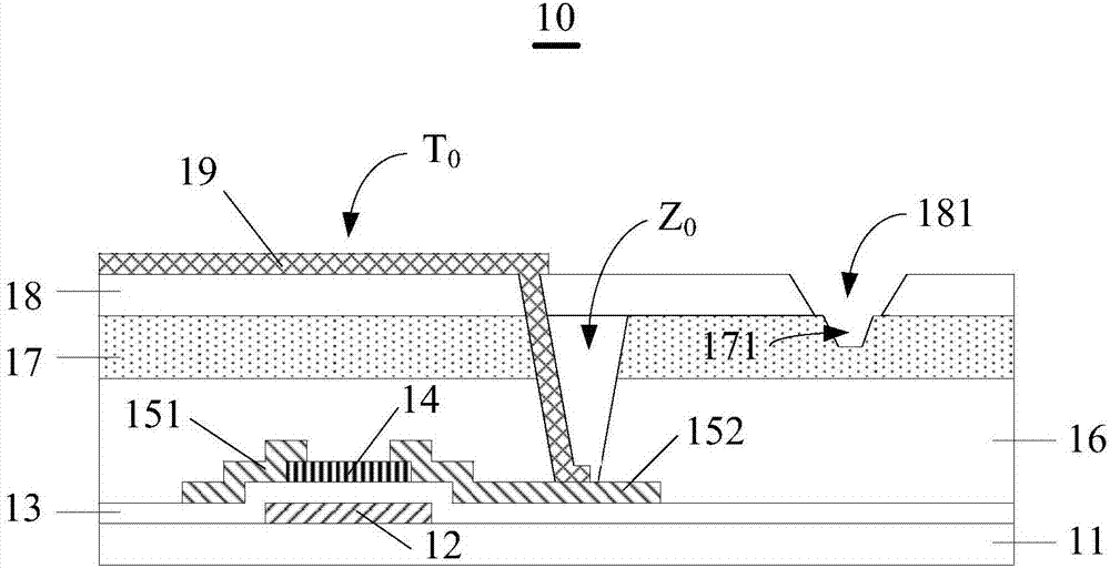
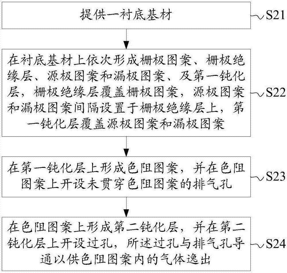
[0023] The main purpose of the present invention is to design the color-resist pattern with vent holes that do not penetrate the color-resist pattern, and to provide via holes in the passivation layer on the color-resist pattern, so that the gas in the color-resist pattern can be released from the vent holes Exhausting through the via hole, the present invention is equivalent to increasing the depth of the exhaust hole, thereby facilitating the discharge of the gas in the color resist pattern and reducing the risk of bubbles in the liquid crystal panel.

[0024] The following will clearly and completely describe the technical solutions of each exemplary embodiment provided by the present invention with reference to the accompanying drawings in the embodiments of the present invention. In the case of no conflict, the following embodiments and technical features thereof can be combined with each other. Moreover, the directional terms used in the following embodiments of the pres...


PUM


Abstract

The invention discloses an array substrate and a manufacturing method thereof and a liquid crystal panel. According to the method, a color ring resistance pattern is designed, and vent holes not running through the color ring resistance pattern are formed, a passivation layer on the color ring resistance pattern is provided with via holes which are communicated with vent holes for gas in the color ring resistance pattern to escape from. Based on this, the array substrate and the manufacturing method thereof and the liquid crystal panel help to discharge the gas inside the color ring resistance pattern and reduce the risk of bubbles appearing on the liquid crystal panel.

Description

technical field [0001] The present invention relates to the field of display technology, in particular to an array substrate, a manufacturing method thereof, and a liquid crystal panel. Background technique [0002] The liquid crystal panel based on COA (Color Filter on Array, color filter array) technology is prone to produce bubbles (bubbles) when it hits. The vias of transistors overlap, and the PV layer (Passivation, passivation layer) at the overlapping position is etched away, causing the gas in the color resistance pattern to precipitate from the overlapping position after the box forming process and form Bubbles. The improvement countermeasure is to expand the color resistance The via size of the pattern makes it not overlap with the TFT via, but this will reduce the penetration rate. The second is that during the vibration process, due to the cracking of the PV layer, the gas in the color resistance pattern is precipitated to form bubbles. The improvement counterme...

Claims


Application Information

Patent Timeline
Patent Type & Authority Applications(China)
IPC IPC(8): G02F1/1362G02F1/1368
CPCG02F1/1362G02F1/136227G02F1/1368G02F1/136222
Inventor 衣志光
Owner TCL CHINA STAR OPTOELECTRONICS TECH CO LTD
Why Eureka
Try Eureka