

Defect inspection and maintenance system, method and maintenance device
A defect detection and maintenance system technology, applied in the direction of measuring devices, measuring electricity, measuring electrical variables, etc., to achieve the effects of convenient maintenance, reducing waste, and improving maintenance efficiency
- Summary
- Abstract
- Description
- Claims
- Application Information
AI Technical Summary
Problems solved by technology
Method used
Image

Examples
Embodiment Construction
[0033] Below, the present invention will be further described in conjunction with the accompanying drawings and specific implementation methods. It should be noted that, under the premise of not conflicting, the various embodiments described below or the technical features can be combined arbitrarily to form new embodiments. .
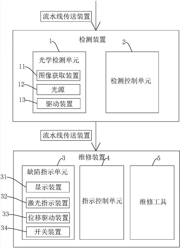
[0034] Such as figure 1 As shown, the present invention provides a defect detection and maintenance system, including a detection device and a maintenance device, wherein the detection device includes an optical detection unit 1 and a detection control unit 2, and the maintenance device includes a defect indication unit 3, an indication control unit 4 and a maintenance tool 5 .
[0035] The optical detection unit 1 is used for taking pictures of the products to be detected entering the detection position of the equipment, so as to obtain images of the products to be detected. The optical detection unit 1 is signal-connected with the detection control...
PUM
 Abstract
Description
Claims
Application Information