Preparation method and equipment of copper-thickening printed circuit board

A printed circuit board, copper thickness technology, applied in the direction of printed circuit manufacturing, printed circuit, removal of conductive materials by chemical/electrolytic methods, etc., can solve problems such as poor tin plating

Inactive Publication Date: 2017-12-19
珠海杰赛科技有限公司 +1
View PDF4 Cites 8 Cited by
  • Summary
  • Abstract
  • Description
  • Claims
  • Application Information

AI Technical Summary

Problems solved by technology

[0019] The embodiment of the present invention provides a method and equipment for preparing copper-thick printed circuit boards, which are used to solve the problem of poor tinning caused by the hidden potion under the dry film during the second copper-tin plating in the prior art The problem

Method used


Image

  • Preparation method and equipment of copper-thickening printed circuit board
  • Preparation method and equipment of copper-thickening printed circuit board
  • Preparation method and equipment of copper-thickening printed circuit board

Examples


Embodiment Construction

[0048] The technical solutions of the present invention will be described in detail below through the accompanying drawings and specific embodiments. It should be understood that the embodiments of the present invention and the specific technical features in the embodiments are only descriptions of the technical solutions of the present invention, rather than limitations. , the embodiments of the present invention and specific technical features in the embodiments may be combined with each other.

[0049] Such as figure 2 Shown is a flow chart of a method for preparing a thick copper printed circuit board in an embodiment of the present invention, the method comprising:

[0050] S201, laminating the printed circuit board;

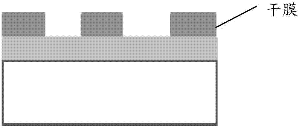
[0051] S202, first attaching a dry film to the surface of the laminated printed circuit board, and performing the first external light imaging;

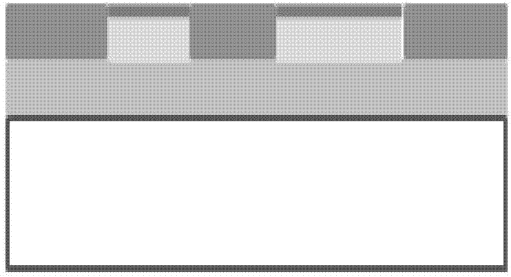
[0052] S203, performing copper thickening treatment on the printed circuit board;

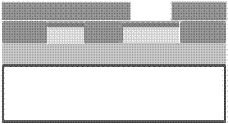
[0053] S204, performing...


PUM


Abstract

The invention discloses a preparation method and equipment of a copper-thickening printed circuit board. After external light imaging is performed for the first time, selective copper thickening treatment is performed firstly, so that the problems in the prior art as follows can be avoided: the lower side wall of a dry film in a winding region in secondary external light imaging suffers from medicinal liquid attack and corrosion to be hollowed out to hide medicinal water, and a poor tin plating phenomenon is caused in the secondary copper plating and tin plating due to the hidden medicinal liquid; by adoption of the preparation method, the selective copper thickening flow is performed on the dry film firstly to satisfy the partial copper thickness requirement; and the subsequent production is performed based on the normal board flow, so that the poor tin plating phenomenon caused by the previous two times of copper plating and tin plating and an open-circuit phenomenon in the subsequent etching can be relieved.

Description

technical field [0001] The present application relates to the field of printed circuit board manufacturing, in particular to a method and equipment for preparing a copper thick printed circuit board. Background technique [0002] The stepped copper thick plate is a stepped copper thick structure realized on the PCB. Its main function is that the local circuit of the circuit board involves high temperature and high pressure conditions during the use process. The ordinary copper thickness is difficult to guarantee the reliability of the use under high temperature and high pressure conditions. Therefore, the copper thickness of the high temperature and high pressure circuit area needs to be designed as thick copper conditions (≥70um) to ensure the reliability when used under high temperature and high pressure conditions, so as to ensure the stable operation of the device and improve the service life. [0003] The existing production process of stepped copper plate is as follows...

Claims


Application Information

Patent Timeline
Patent Type & Authority Applications(China)
IPC IPC(8): H05K3/06
CPCH05K3/064H05K2203/052H05K2203/0551H05K2203/1476
Inventor 李思周郑凡王力覃立张良昌宁武珍
Owner 珠海杰赛科技有限公司
Why Eureka
Try Eureka