Array substrate and display panel

An array substrate, electrostatic technology, applied in optics, instruments, electrical components, etc., can solve the problems of no anti-static unit design on the array substrate, lower product yield, damage to the display area, etc., to improve the anti-ESD ability, improve product quality quality effect

Active Publication Date: 2017-12-22
WUHAN CHINA STAR OPTOELECTRONICS TECH CO LTD
View PDF3 Cites 8 Cited by
  • Summary
  • Abstract
  • Description
  • Claims
  • Application Information

AI Technical Summary

Problems solved by technology

[0006] The existing array substrate does not have an anti-static unit, and the gate wiring layer is easy to attract circuits. Once a row of gates generates static electricity, there is nowhere to release the static electricity, which will lead to damage to the Pixel (pixel) in the display area or the GOA circuit. Injury, which will eventually affect the normal function of the panel and reduce the yield of the product

Method used


Image

  • Array substrate and display panel
  • Array substrate and display panel
  • Array substrate and display panel

Examples


Embodiment Construction

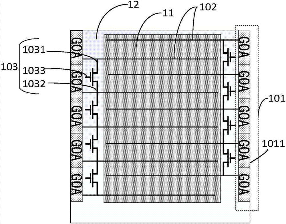
[0025] refer to figure 1 , figure 1 It is a structural schematic diagram of the first embodiment of the array substrate of the present invention.

[0026] like figure 1 As shown, the array substrate is divided into a display area 11 and a non-display area 12 . The array substrate includes a GOA unit 101, a plurality of gate signal lines 102 and an electrostatic conduction device. Further, the GOA unit 101 includes several GOA subunits 1011 , and the gate signal line 102 is electrically connected to the several GOA subunits 1011 one by one. The electrostatic conduction device is electrically connected between the plurality of gate signal lines 102, so that the gate signal lines 102 are electrically connected to each other. It should be noted that, in this embodiment, the GOA units are distributed on both sides of the array substrate. In other embodiments, the GOA units may also be distributed on only one side of the array substrate, which is not limited in the present inven...


PUM


Abstract

The invention discloses an array substrate and a display panel. The array substrate comprises a GOA (gate driver on array) unit, a plurality of grid signal lines and electrostatic conduction devices. The grid signal lines are electrically connected with the GOA unit, and the electrostatic conduction devices are electrically connected among the grid signal lines to realize electrical connection of the grid signal lines. The array substrate has advantages that by the electrostatic conduction devices among the grid signal lines, the grid signal lines are connected together to jointly resist ESD (electrostatic discharge), and accordingly ESD resistance of the array substrate can be evidently improved, and product quality is improved.

Description

technical field [0001] The present invention relates to the field of display technology, in particular to an array substrate and a display panel. Background technique [0002] During the production process of the display panel, due to some external factors, such as continuous process operation and handling or environmental changes, etc., electrostatic charges usually accumulate in the panel. Since glass itself is an insulating substance, unless there is a proper discharge path, static charges will remain on the surface of the substrate. When the electrostatic charge accumulates to a certain amount, a discharge (ESD, Electrostatic Discharge) will occur. [0003] The time when electrostatic discharge occurs is very short, and the transfer of a large amount of charges in a short time will generate extremely high current, break down semiconductor devices, or generate enough heat to melt semiconductor devices. This kind of hazard is usually not easy to detect. Under the circums...

Claims


Application Information

Patent Timeline
Patent Type & Authority Applications(China)
IPC IPC(8): G02F1/1362H01L27/02H01L27/12
CPCG02F1/136204G02F2202/22H01L27/0292H01L27/124G02F1/13454H01L27/0288H01L27/0296G02F1/136286
Inventor 洪光辉
Owner WUHAN CHINA STAR OPTOELECTRONICS TECH CO LTD
Why Eureka
Try Eureka