Broadband electromagnetic transparent enhancement device
An enhancement device and electromagnetic technology, applied in the direction of electrical components, antennas, etc., can solve the problems of complex processing, complex design structure, increased loss, etc., and achieve the effect of wide frequency range, reduced strength, and enhanced transmittance
- Summary
- Abstract
- Description
- Claims
- Application Information
AI Technical Summary
Problems solved by technology
Method used
Image

Examples
Embodiment Construction
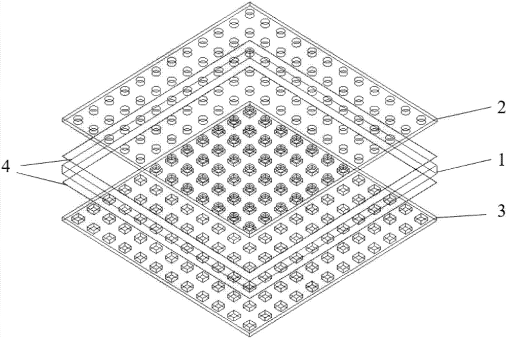
[0016] Such as figure 1 As shown in the schematic diagram of the overall structure development of the broadband electromagnetic transparency enhancement device, a weak electromagnetic transparent material 1, a first electromagnetic anti-reflection plate 2, a second electromagnetic anti-reflection plate 3 and glue 4; the thickness of the weak electromagnetic transparent material 1 5mm, the relative dielectric constant is 7.0, and the loss tangent is 0.05; the thickness of the first electromagnetic anti-reflection plate is 1.5mm, and it is pasted on the front of the weak electromagnetic transparent material 1 through the glue 4; the second electromagnetic anti-reflection plate The thickness of the transparent plate is 1.4mm, and it is pasted on the reverse side of the weak electromagnetic material 1 through the glue 4;
[0017] Further, the relative dielectric constant of the dielectric material used in the first electromagnetic anti-reflection board 2 is 6.15, and the loss tang...
PUM
 Abstract
Description
Claims
Application Information