Scribing groove test structure and test method thereof

A technology of test structure and test method, applied in the direction of semiconductor/solid-state device test/measurement, electrical components, electrical solid-state devices, etc., can solve the problems that the dicing groove cannot be further narrowed, restrict the integration of chips, etc., and achieve significant technical effects , improve the effect of integration

Active Publication Date: 2017-12-26
SHANGHAI HUAHONG GRACE SEMICON MFG CORP
View PDF6 Cites 9 Cited by
  • Summary
  • Abstract
  • Description
  • Claims
  • Application Information

AI Technical Summary

Problems solved by technology

[0003] However, with the improvement of chip integration, the output of chips per unit area is getting higher and higher, which promotes the development of scribing grooves between chips in a narrower and narrower direction. The size of the test structure pad is restricted. For

Method used


Image

  • Scribing groove test structure and test method thereof

Examples


Embodiment Construction

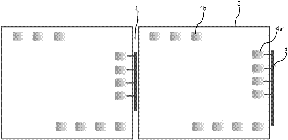
[0028] Such as figure 1 As shown, it is a schematic diagram of the scribe groove test structure of the embodiment of the present invention. In the scribe groove test structure of the embodiment of the present invention, the chip formation area 2 and the scribe groove 1 are included on the same wafer. figure 1 Only two chip formation regions 2 are shown in , but actually there are chip formation regions 2 on the same wafer, and the higher the chip integration degree, the more chip formation regions 2 are.

[0029] The test structure 3 is formed in the scribe groove 1 .

[0030] The first pad 4a of the test structure 3 is formed in the chip formation area 2 and formed by patterning the top front metal layer.

[0031] The test structure 3 is connected to the first pad 4a through more than one front metal layer and corresponding contact holes.

[0032] Depend on figure 1 As shown, since the first pad 4a no longer covers the scribe groove 1 in the embodiment of the present inven...


PUM

PropertyMeasurementUnit
Sizeaaaaaaaaaa
Side lengthaaaaaaaaaa

Abstract

The invention discloses a scribing groove test structure. A same wafer comprises a chip formation area and a scribing groove. The test structure is formed in the scribing groove. A first bonding pad of the test structure is formed in the chip formation area and is formed through diagramming a top-layer front-side metal layer. Through more than one front-side metal layer and a corresponding contact hole, the test structure is connected to the first bonding pad. A width of the scribing groove is less than a size of the first bonding pad in the narrowest position. Through setting the first bonding pad in the chip formation area, the width of the scribing groove is not influenced by the size of the first bonding pad so that the size of the scribing groove is reduced and an integrated level of a chip on the wafer is increased. The invention also discloses a test method of the scribing groove test structure. The integrated level of the chip can be increased and cost is reduced.

Description

technical field [0001] The invention relates to the field of semiconductor integrated circuit manufacturing, in particular to a scribe groove test structure. The invention also relates to a test method for the scribe groove test structure. Background technique [0002] In the integrated circuit manufacturing process, multiple chips are integrated on the same wafer (wafer). The wafer is generally a silicon substrate wafer, and a dicing groove is formed between the chips. After the wafer is manufactured, Chips are separated by dicing the scribe slots. In the chip manufacturing process, it is often necessary to test the chip, and a test structure needs to be specially designed to monitor the production situation. Since the test structure is only useful during the test process and is no longer used after the test is completed, the test structure is usually set in In the dicing groove, so as not to occupy the area of ​​the chip, so as to improve the integration level. [0003]...

Claims


Application Information

Patent Timeline
IPC IPC(8): H01L23/544H01L21/66
CPCH01L23/544H01L22/20
Inventor 吴苑曾志敏
Owner SHANGHAI HUAHONG GRACE SEMICON MFG CORP
Why Eureka
Try Eureka