Wafer laser marking technology implementation method and system based on CAD (computer aided design)
A computer-aided, laser marking technology, applied in the directions of calculation, design optimization/simulation, special data processing applications, etc., can solve the problem of increasing the difficulty of laser marking process development
- Summary
- Abstract
- Description
- Claims
- Application Information
AI Technical Summary
Problems solved by technology
Method used
Image

Examples
Embodiment 1
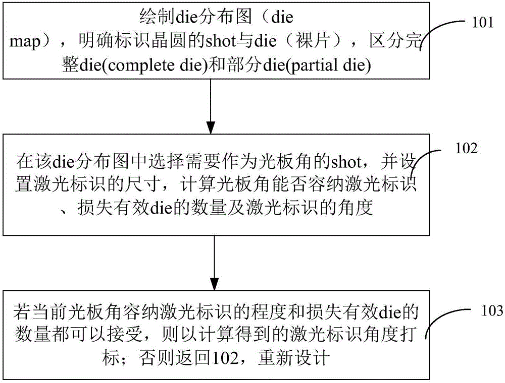
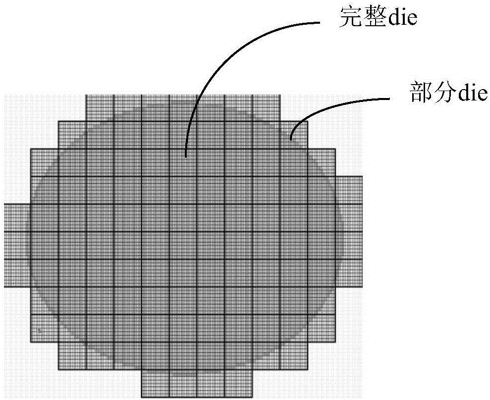
[0065] After the first round of design, the corner of the light board can accommodate the laser mark (laser mark), and lose 8 complete dies (complete die); the customer decided to adopt this design, so the laser mark angle is determined to be 52 degrees. Such as Figure 8-1 shown.
Embodiment 2
[0067] After the first round of design, the corner of the bare board could not accommodate the laser mark, and 21 complete dies (complete die) were lost; but the chord length was 17.14mm, and at most one character was typed outside the corner of the bare board. After weighing, the customer decided to still adopt this design, so The laser mark angle is determined to be 55 degrees, such as Figure 8-2 shown.
Embodiment 3
[0069] After the first round of design, the corner of the bare board could not accommodate the laser mark, 6 complete dies (complete die) were lost, the chord length was 10.81mm, and at least four characters were typed outside the corner of the bare board, which may affect character recognition. On balance, the client decided to redesign. Such as Figure 8-3 shown.
[0070] After the second round of design, the corner of the light board can accommodate the laser mark, and 26 completeddies are lost; the customer decided to adopt this design, so the angle of the laser mark is determined to be 126 degrees. Such as Figure 8-4 shown.
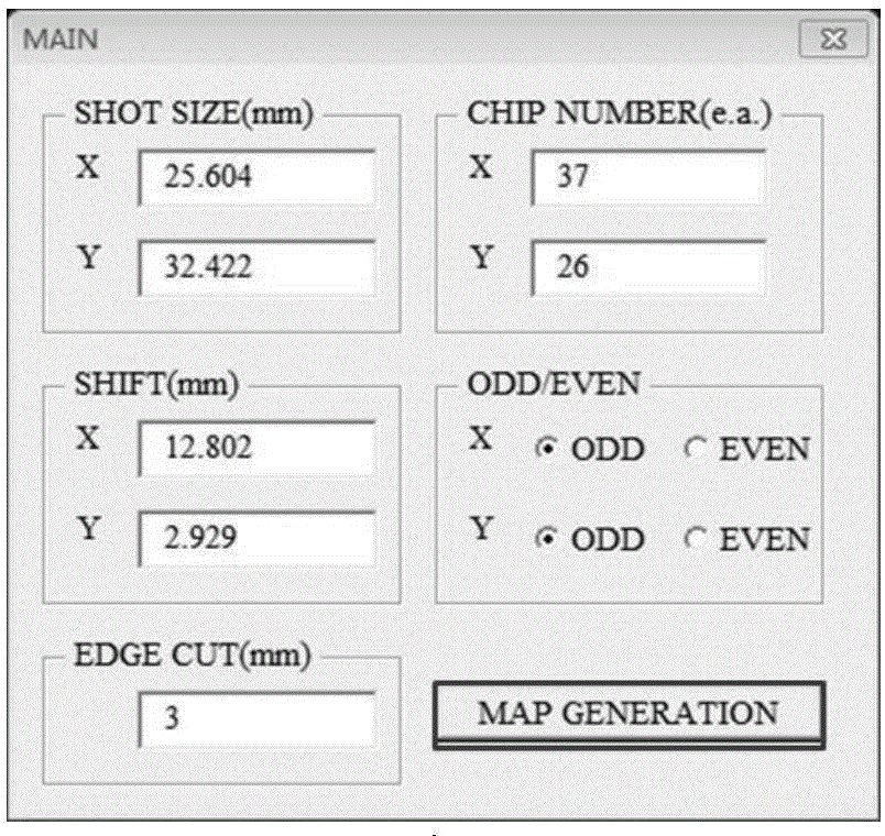
[0071] Figure 9 It is a system architecture diagram of a computer-aided design-based wafer laser marking process realization system of the present invention. Such as Figure 9 As shown, a computer-aided design-based wafer laser marking process implementation system of the present invention includes: a die distribution diagram drawing unit 901...
PUM
 Abstract
Description
Claims
Application Information
 - R&D
- Intellectual Property
- Life Sciences
- Materials
- Tech Scout
- Unparalleled Data Quality
- Higher Quality Content
- 60% Fewer Hallucinations
Browse by: Latest US Patents, China's latest patents, Technical Efficacy Thesaurus, Application Domain, Technology Topic, Popular Technical Reports.
© 2025 PatSnap. All rights reserved.Legal|Privacy policy|Modern Slavery Act Transparency Statement|Sitemap|About US| Contact US: help@patsnap.com