Novel through hole structure
A via hole, a new type of technology, applied in the direction of printed circuit components, etc., can solve the problems of occupied board area, single signal quality impact, limited space, etc., to achieve increased parasitic inductance, reduced usage and occupied area , the effect of discontinuity reduction
- Summary
- Abstract
- Description
- Claims
- Application Information
AI Technical Summary
Problems solved by technology
Method used
Image
Examples
Embodiment Construction
[0022] In order to make the technical problems, technical solutions and beneficial effects to be solved by the present invention clearer, the present invention will be described in detail below in conjunction with the accompanying drawings and embodiments. It should be noted that the specific embodiments described here are only used to explain the present invention, not to limit the present invention.
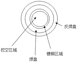
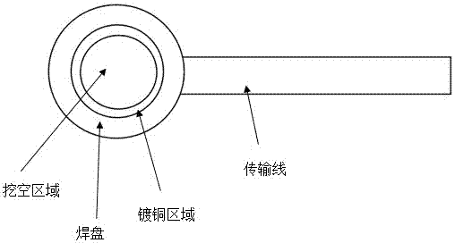
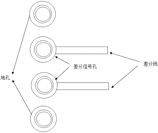
[0023] The new via structure is composed of a signal area and a ground area. The signal area and the ground area are isolated by an isolation area. Hollow areas are provided on both sides of the isolation area. The signal area and the ground area are respectively located in the excavated On the outside of the empty area, anti-pads are provided outside the signal area and the ground area; the signal area can be connected to a single signal line or a differential signal line, and the signal part and the ground part of the via are respectively located on the two sides of the via. ...
PUM
 Abstract
Description
Claims
Application Information


