Array substrate and method for manufacturing the same, and method for improving adhesiveness between film layers

A technology for array substrates and manufacturing methods, which is applied in the field of thin film manufacturing, can solve problems such as disconnection, peeling of source and drain metal layers, and affecting the yield of array substrates, and achieve the effect of improving yield

Inactive Publication Date: 2018-01-16
SHENZHEN CHINA STAR OPTOELECTRONICS TECH CO LTD
View PDF8 Cites 2 Cited by
  • Summary
  • Abstract
  • Description
  • Claims
  • Application Information

AI Technical Summary

Problems solved by technology

[0003] However, in the process of manufacturing the semiconductor material layer and the source-drain metal layer, due to the poor adhesion between the semiconductor material layer and the source-drain metal layer, the source-drain metal layer will be peeled off, resulting in a disconnection problem, and then Affect the yield of array substrate

Method used


Image

  • Array substrate and method for manufacturing the same, and method for improving adhesiveness between film layers
  • Array substrate and method for manufacturing the same, and method for improving adhesiveness between film layers

Examples


Embodiment Construction

[0019] Hereinafter, embodiments of the present invention will be described in detail with reference to the accompanying drawings. This invention may, however, be embodied in many different forms and should not be construed as limited to the specific embodiments set forth herein. Rather, the embodiments are provided to explain the principles of the invention and its practical application, thereby enabling others skilled in the art to understand the invention for various embodiments and with various modifications as are suited to particular intended uses.

[0020] In the drawings, the thicknesses of layers and regions are exaggerated for clarity. Like reference numerals refer to like components throughout the specification and drawings.

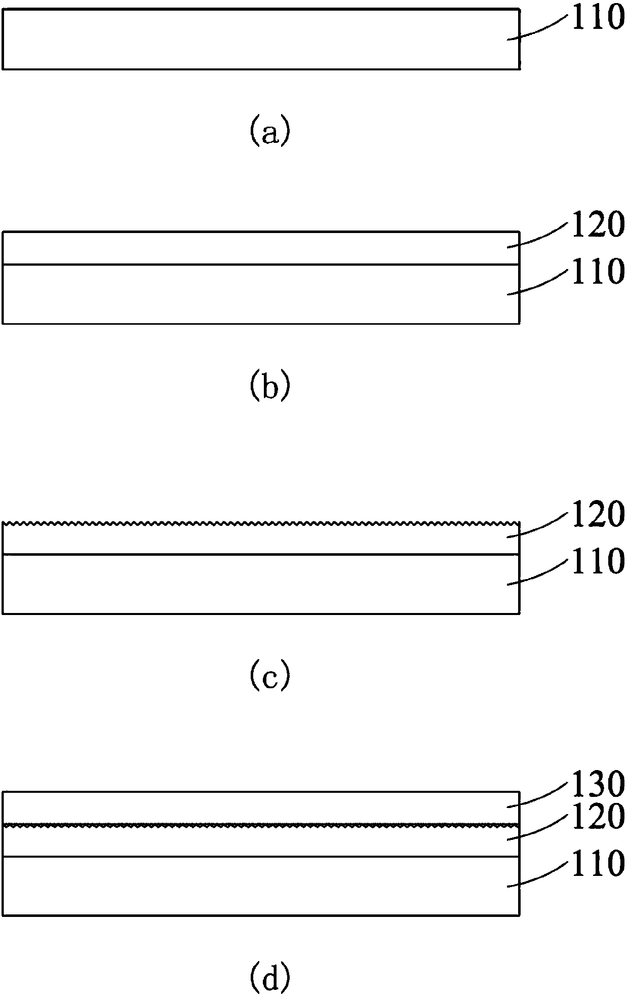
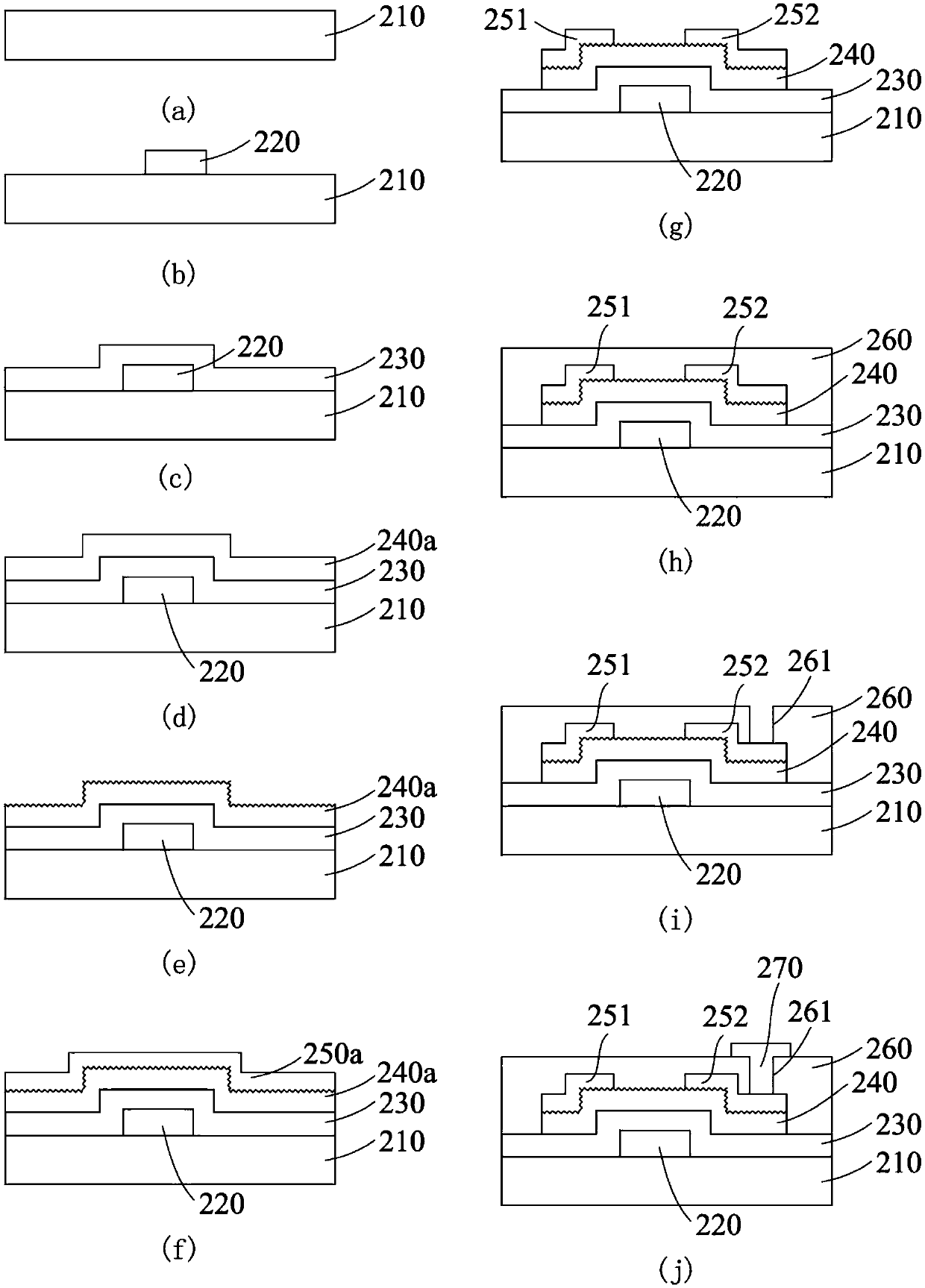
[0021] figure 1 is a process chart of a method for improving the adhesion between film layers according to an embodiment of the present invention.

[0022] The method for improving the adhesion between film layers according to an embodiment ...


PUM


Abstract

The invention provides a method for manufacturing an array substrate. The method comprises: providing a substrate; forming a gate on the substrate; forming a gate insulating layer on the substrate andthe gate; forming a semiconductor material layer on the gate insulating layer; carrying out roughening processing on the surface of the semiconductor material layer; forming source-drain metal layeron the semiconductor material layer; carrying out exposing, developing, and etching on the source-drain metal layer and the semiconductor material layer so as to form an active layer on the gate insulating layer and form a source and a drain that are spaced from each other on the active layer and the gate insulating layer; forming a passivation layer on the active layer, the gate insulating layer,the source and the drain; forming a via hole exposing the drain electrode; and forming a pixel electrode in contact with the drain through the via hole on the passivation layer. According to the invention, because roughening processing is carried out on the surface of the active layer, the adhesive forces of the source, the drain, and the active layer are strengthened, thereby avoiding line breaking and improving the yield of the array substrate.

Description

technical field [0001] The invention belongs to the technical field of film production, and in particular relates to an array substrate and a production method thereof, and a method for improving the adhesion between film layers. Background technique [0002] At present, the array substrate in the liquid crystal panel can be manufactured using the 4Mask process. When making the active layer and the source and drain electrodes, the gate insulating layer, the semiconductor material layer and the source and drain metal layers are formed first, and then the mask process is used to form the active layer at the same time. source layer and source drain. [0003] However, in the process of manufacturing the semiconductor material layer and the source-drain metal layer, due to the poor adhesion between the semiconductor material layer and the source-drain metal layer, the source-drain metal layer will be peeled off, resulting in a disconnection problem, and then affect the yield of ...

Claims


Application Information

Patent Timeline
Patent Type & Authority Applications(China)
IPC IPC(8): H01L21/77H01L27/12
Inventor 高冬子
Owner SHENZHEN CHINA STAR OPTOELECTRONICS TECH CO LTD
Why Eureka
Try Eureka