

Illumination system of projection exposure equipment for microlithography
A lighting system and microlithography technology, applied in the field of lighting systems, can solve the problems of increasing the complexity and cost of the complete system
- Summary
- Abstract
- Description
- Claims
- Application Information
AI Technical Summary
Problems solved by technology
Method used
Image

Examples
Embodiment Construction
[0064] I. Conventional Construction of Projection Exposure Equipment
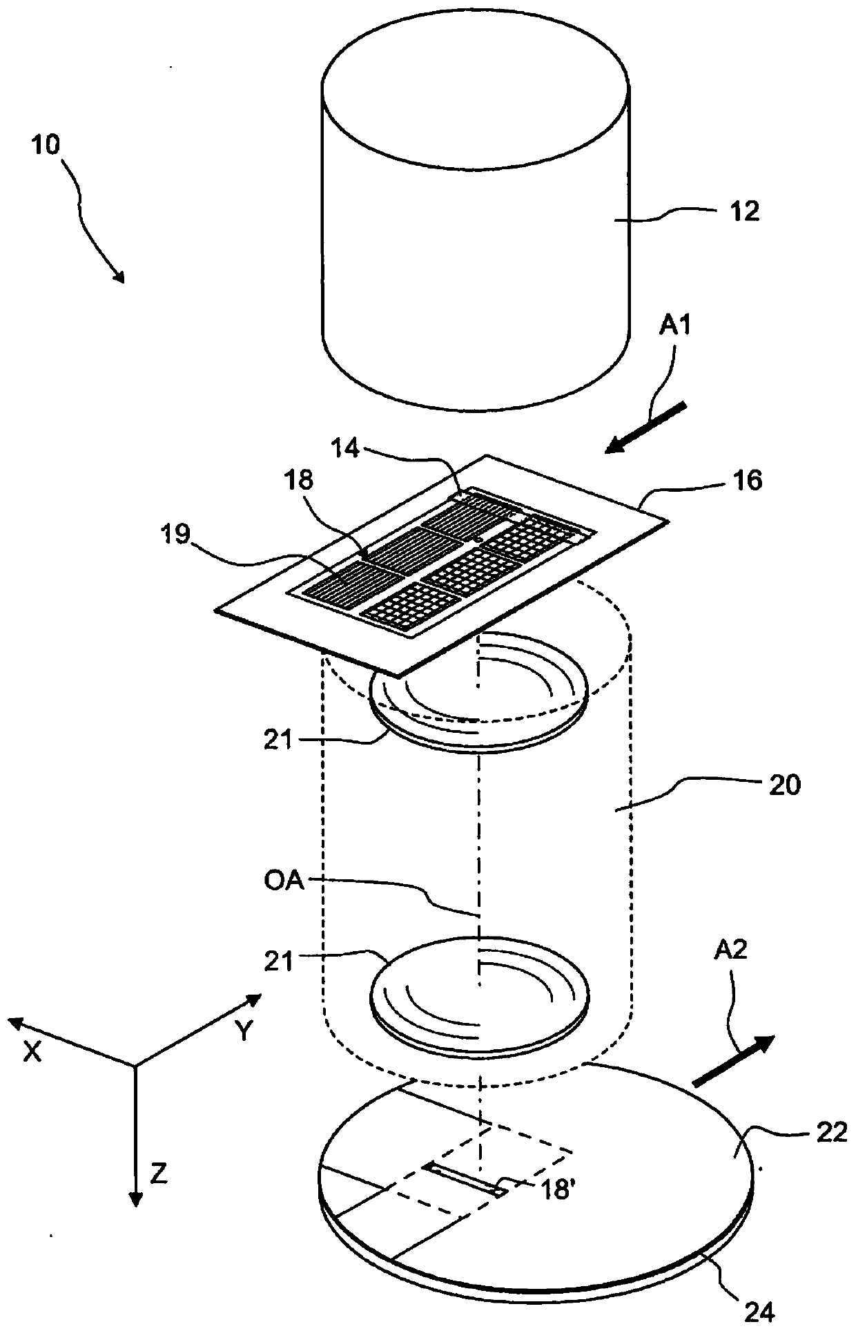
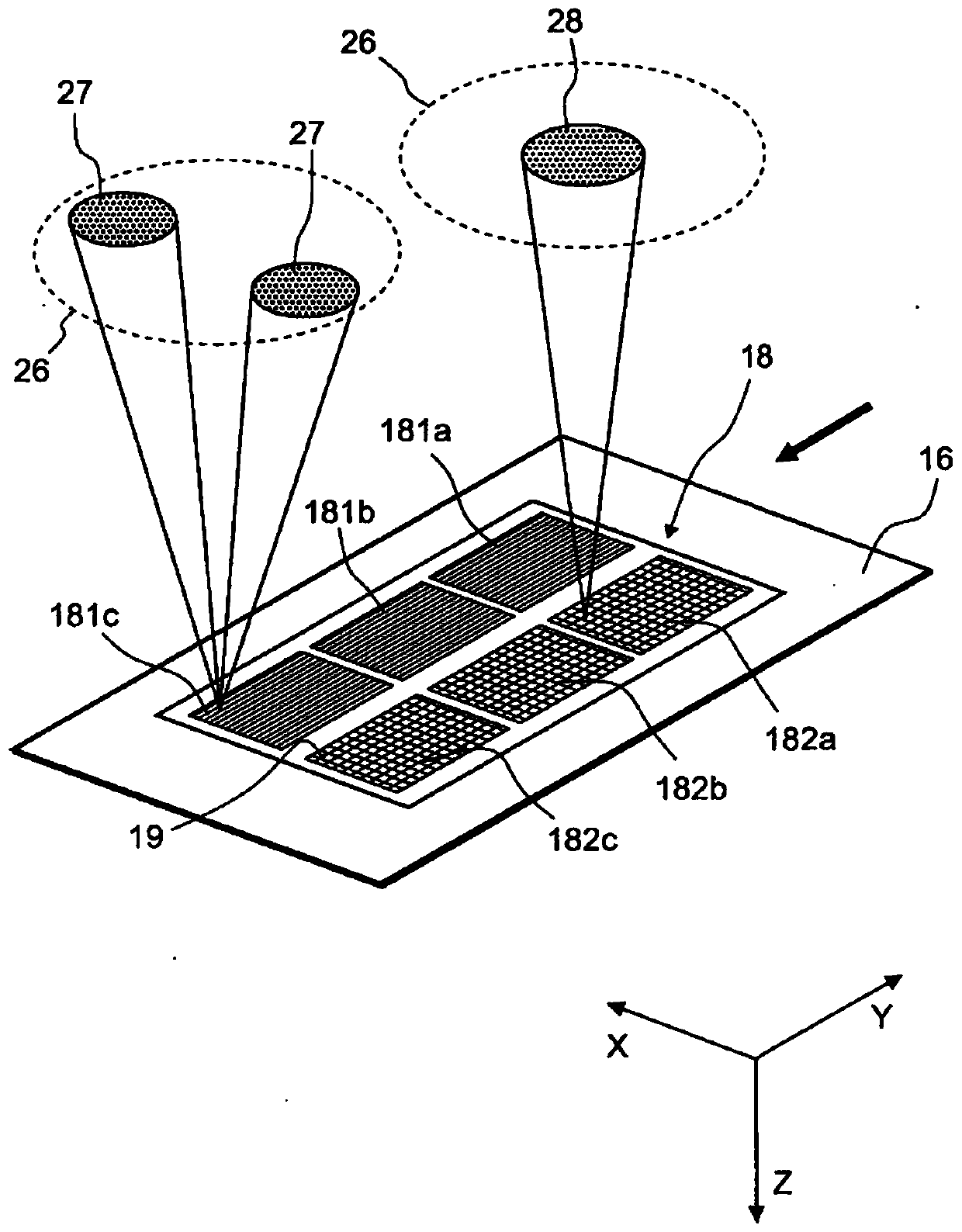
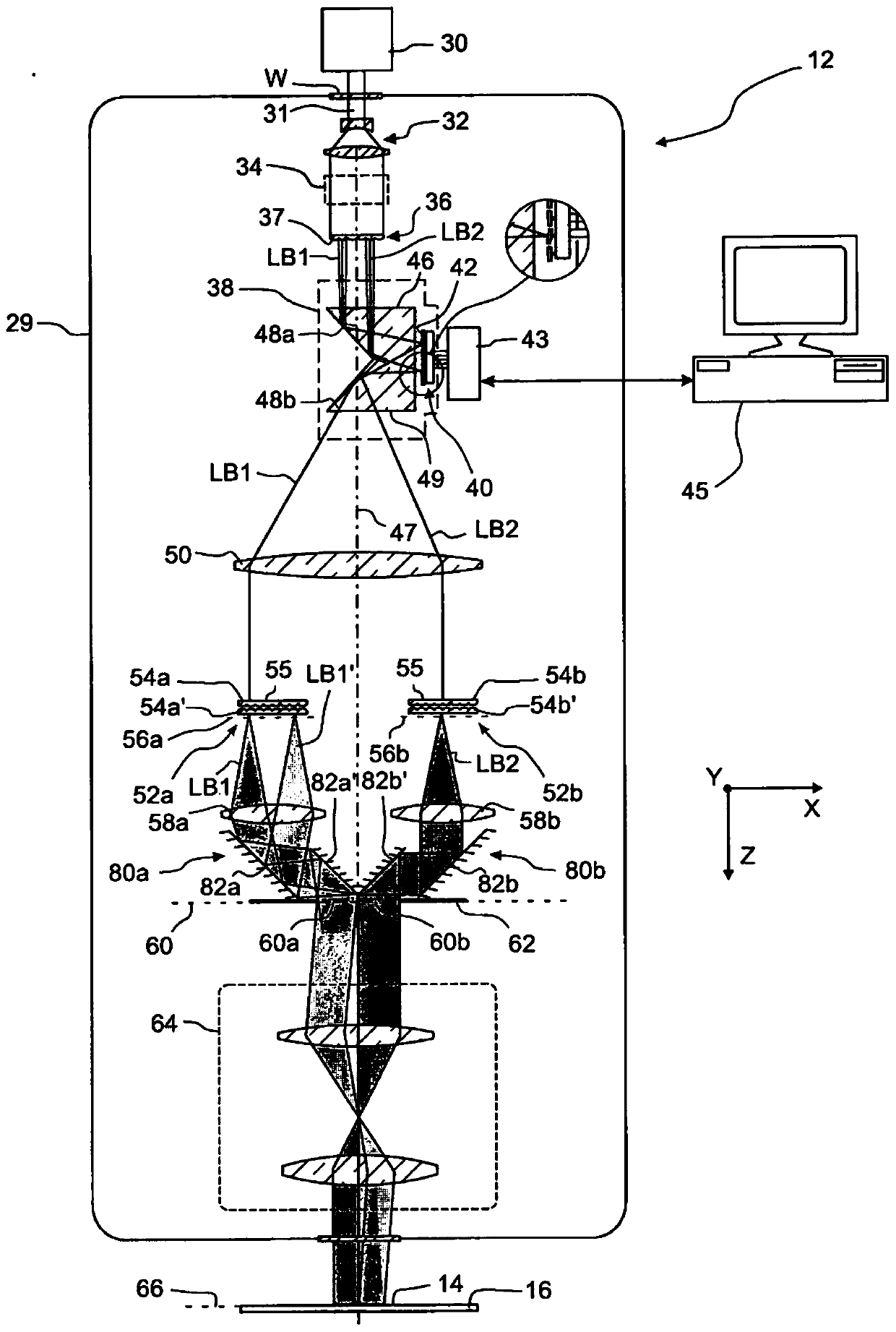
[0065] figure 1 is a perspective and highly simplified view of a projection exposure apparatus 10 according to the invention. The device 10 includes an illumination system 12 which generates a projected light beam. The latter illuminates a field 14 on a mask 16 containing a pattern 18 of fine features 19 . In this embodiment, the illuminated field 14 has a rectangular shape. However, other shapes of the illumination field 14, for example ring segments, are also conceivable.
[0066] The projection objective 20 has an optical axis OA and comprises a plurality of lenses 21 , imaging the pattern 18 within the illuminated field 14 onto a photosensitive layer 22 , such as photoresist, which is supported by a substrate 24 . A substrate 24 , which may be formed by a silicon wafer, is arranged on a wafer stage (not shown) such that the top surface of the photosensitive layer 22 lies precisely within the image p...
PUM
 Abstract
Description
Claims
Application Information