A device for realizing clock and reset control chip working mode

A working mode and reset control technology, which is applied in the direction of logic circuit connection/interface layout, etc., can solve the problem that it is impossible to add an external pin PAD_IO, etc., and achieve the effect of ensuring safety certification, good compatibility, and easy transplantation

Active Publication Date: 2020-10-02
SHANGHAI INTEGRATED CIRCUIT RES & DEV CENT +1
View PDF4 Cites 0 Cited by
  • Summary
  • Abstract
  • Description
  • Claims
  • Application Information

AI Technical Summary

Problems solved by technology

[0004] However, the external pin PAD_IO of mass-produced chips in the industry is a precious resource, especially for the benchmark chip, it is impossible to add a new external pin PAD_IO when implementing the DFT test function.

Method used


Image

  • A device for realizing clock and reset control chip working mode

Examples


Embodiment Construction

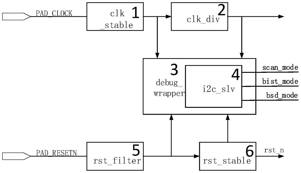
[0028] Attached below figure 1 , the specific embodiment of the present invention will be further described in detail.

[0029] It is clear to those skilled in the art that almost all digital circuit chips have clock PAD_CLOCK input pins and reset PAD_RESETN control pins, and the present invention only uses clocks and resets to control the chip operating mode (i.e. the selection of general operating mode and / or DFT operating mode) Switching) will not increase the associated costs, nor will it affect compatibility.

[0030] see figure 1 , figure 1 Shown is a block diagram of a device for realizing the working mode of the clock and reset control chip of the present invention. As shown in the figure, in addition to using the clock PAD_CLOCK input pin and the reset PAD_RESETN control pin, the implementation device also includes a clock stabilization circuit module clk_stable 1, a frequency division module clk_div 2, a filter circuit rst_filter 5, a debug controller debug_wrappe...


PUM


Abstract

The invention provides a device for implementing a clock and reset control chip working mode, which is used for selecting and switching a universal working mode and / or a DFT working mode; the device comprises a clock PAD-CLOCK input pin and a reset PAD-RESETN control pin, wherein the device further comprises a clock stabilizing circuit module clk-stable, a frequency division module clk-div, a filtering circuit rst-filter, a debugging controller debug-wrappper and a reset stabilizing circuit module rst-stable, the debugging controller debug-wrappper comprises a state corresponding table and ani2c-slv logic unit. Therefore, the device only uses the clock PAD-CLOCK input pin and the reset PAD-RESETN control pin to realize the control chip working mode, filters unnecessary reset pulses on thepremise of stable input clock to obtain expected input, and obtains a stable control signal via the i2c-slv protocol, so that the chip works in a specific mode.

Description

technical field [0001] The invention relates to the technical field of integrated circuits, in particular to the logic design of chip hardware, and in particular to a device for realizing clock and reset control chip working modes. Background technique [0002] The working modes of semiconductor chips can be divided into: ordinary (various functions), design for testability (Design for Testability, referred to as DFT) mode), DFT mode is a kind of integrated circuit design technology, DFT working mode usually includes scan_mode, bist_mode, bsd_mode And / or bypass_mode, which implants some special structures into the circuit during the design stage, so that it can be tested after the design is completed. However, it is sometimes not easy to test the internal circuit of a semiconductor chip, because many internal node signals of the circuit are difficult to test and control externally, usually by adding testability design structures, such as scan chains, etc., internal signals c...

Claims


Application Information

Patent Timeline
Patent Type & Authority Patents(China)
IPC IPC(8): H03K19/0175
Inventor 李林张小亮张远袁庆史汉臣李琛温建新
Owner SHANGHAI INTEGRATED CIRCUIT RES & DEV CENT
Why Eureka
Try Eureka