Apparatus and method for polishing a surface of a substrate

A technology for grinding substrates and substrates, which is applied in the field of surface devices, can solve the problems of excessive wafer grinding, residual foreign matter, grinding, etc., and achieve the effect of reducing the grinding process

Active Publication Date: 2018-01-26
EBARA CORP
View PDF8 Cites 7 Cited by
  • Summary
  • Abstract
  • Description
  • Claims
  • Application Information

AI Technical Summary

Problems solved by technology

However, since the amount of foreign matter varies from wafer to wafer, grinding for a certain grinding time sometimes produces over-grinding and / or undergrinding of the wafer.
That is, foreign matter may remain on a certain wafer, and the wafer may be excessively chipped on another wafer

Method used


Image

  • Apparatus and method for polishing a surface of a substrate
  • Apparatus and method for polishing a surface of a substrate
  • Apparatus and method for polishing a surface of a substrate

Examples


Embodiment Construction

[0095] Hereinafter, embodiments of the present invention will be described with reference to the drawings.

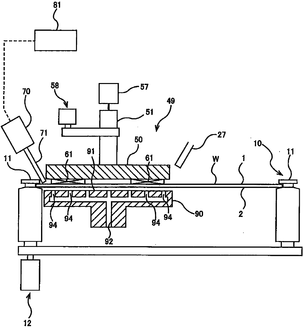
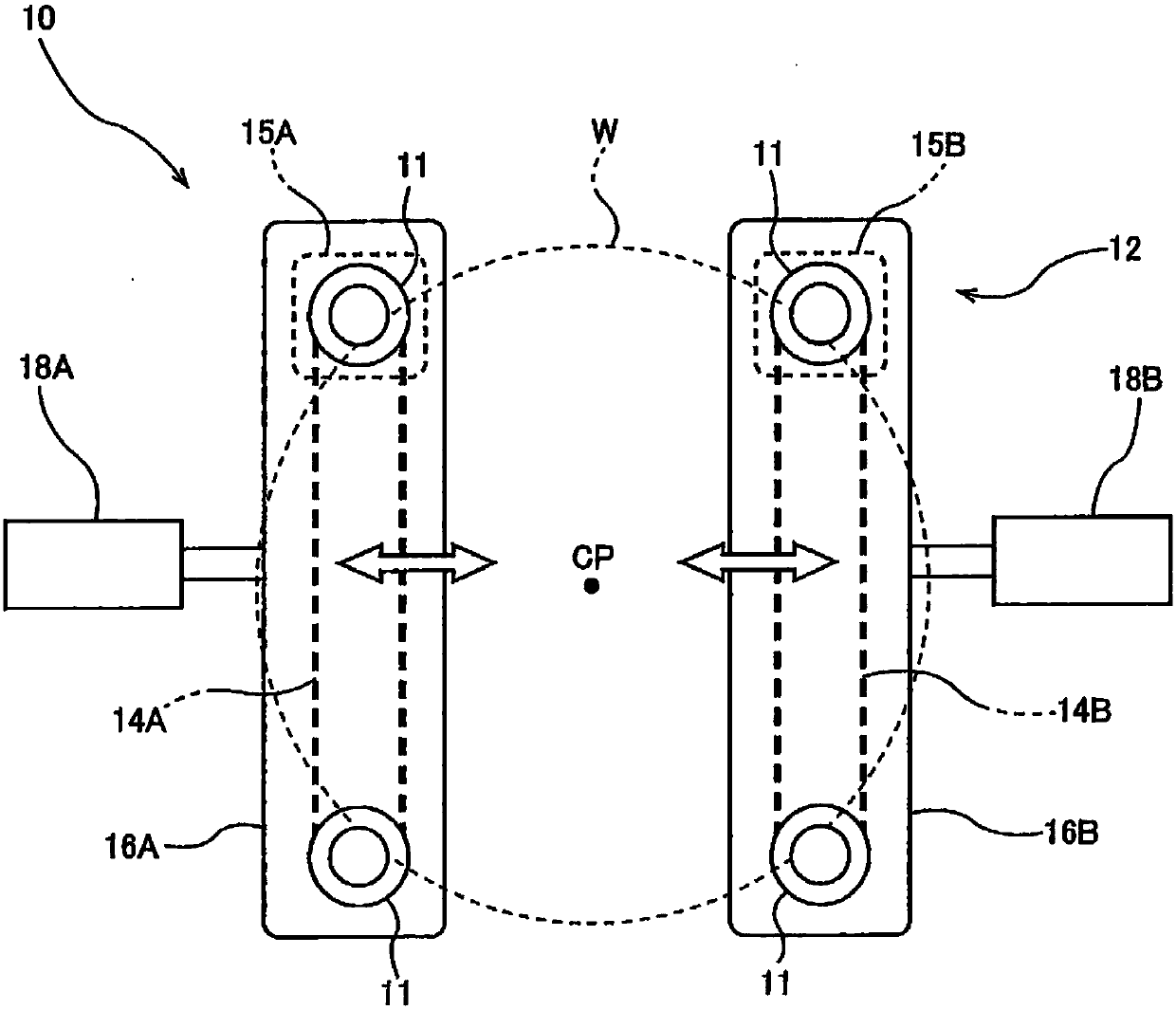
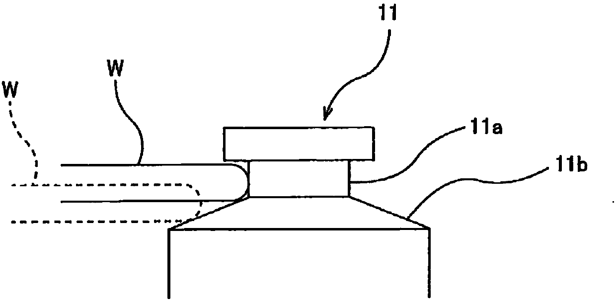
[0096] figure 1 It is a schematic diagram showing an embodiment of a polishing apparatus. The polishing apparatus includes a substrate holding portion 10 that holds a wafer W as an example of a substrate and rotates the wafer W around its axis; a polishing head assembly 49 that holds Polishing is performed on the first surface 1 of the wafer W of the substrate holding portion 10 to remove foreign matter and scratches from the first surface 1 of the wafer W; and a static pressure support table 90 as a substrate support table, which is opposed to The second surface 2 of the wafer W on the side opposite to the first surface 1 supports. The polishing head assembly 49 is arranged on the upper side of the wafer W held by the substrate holding portion 10, and the hydrostatic support table 90 is arranged on the lower side of the wafer W held by the substrate holding portion 10.

...


PUM


Abstract

The invention provides an apparatus for polishing a surface of a substrate. The entire surface of a substrate, such as a wafer, can be polished, and the outermost part of the surface of the substratecan be polished without using an edge polishing device, so that the polishing process is reduced. The apparatus includes a substrate holder (10) configured to hold a substrate (W) and rotate the substrate (W); and a polishing head (50) configured to rub a polishing tool (61) against a first surface (1) of the substrate (W) to polish the first surface (1). The substrate holder (10) includes a plurality of rollers (11) which can contact a periphery of the substrate (W). The plurality of rollers (11) are rotatable about their respective own axes.

Description

Technical field [0001] The present invention relates to an apparatus and method for polishing the surface of a substrate such as a wafer. Background technique [0002] In recent years, devices such as memory circuits, logic circuits, and image sensors (such as CMOS sensors) have been increasingly integrated. In the process of forming these devices, foreign matter such as particles and dust may adhere to the devices. Foreign matter adhering to the device can cause short circuits between wiring and circuit defects. Therefore, in order to improve the reliability of the device, it is necessary to clean the wafer on which the device is formed and remove foreign matter on the wafer. [0003] The back surface (non-device surface) of the wafer may also adhere to foreign matter such as fine particles and dust as described above. If such foreign matter adheres to the back surface of the wafer, the wafer is separated from the stage reference surface of the exposure apparatus or the wafer s...

Claims


Application Information

Patent Timeline
Patent Type & Authority Applications(China)
IPC IPC(8): B24B37/013B24B37/04
Inventor 石井游中西正行内山圭介
Owner EBARA CORP
Why Eureka
Try Eureka