A time amplifier and a semiconductor memory

A time amplifier, the technology of the first time, applied in the direction of amplification control, electrical components, gain control, etc., can solve the problems of low measurement accuracy, time amplification gain can not be adjusted according to actual needs, etc., to achieve adjustable gain, The effect of increasing the amplification gain

Active Publication Date: 2018-02-02
CHANGXIN MEMORY TECH INC
View PDF8 Cites 2 Cited by
  • Summary
  • Abstract
  • Description
  • Claims
  • Application Information

AI Technical Summary

Problems solved by technology

Among them, the SR latch-based time amplifier consists of two SR latches and a gate, and its gain is proportional to the additional capacitance set at the output of the SR latch, however, the SR latch-based time amplifier’s The main disadvantage is that the gain of time amplification cannot be adjusted according to actual needs, which leads to low accuracy of time interval measurement of DLL

Method used


Image

  • A time amplifier and a semiconductor memory
  • A time amplifier and a semiconductor memory
  • A time amplifier and a semiconductor memory

Examples


Embodiment 1

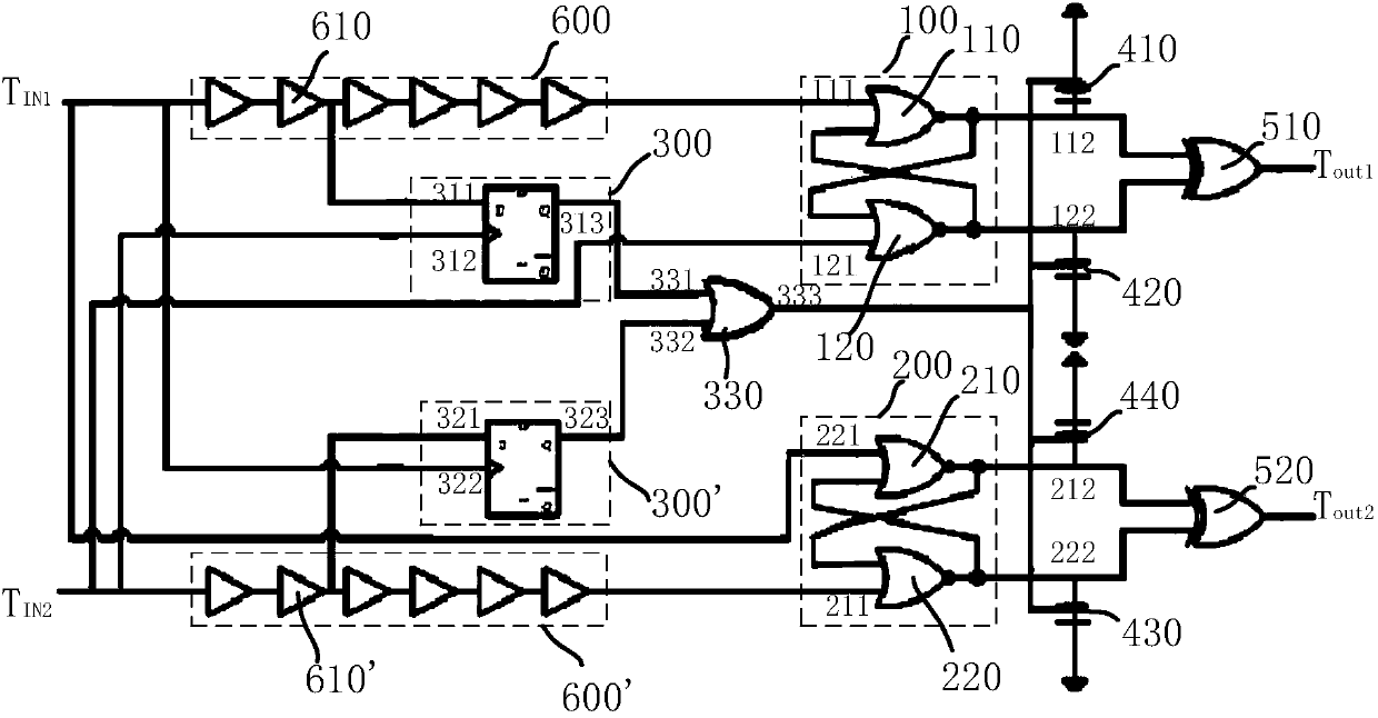
[0062] In a specific implementation, a time amplifier is provided, including:

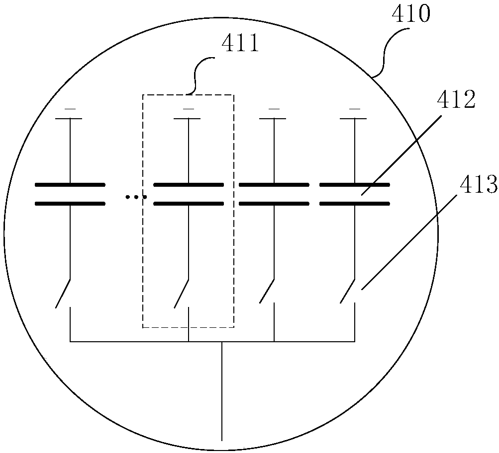
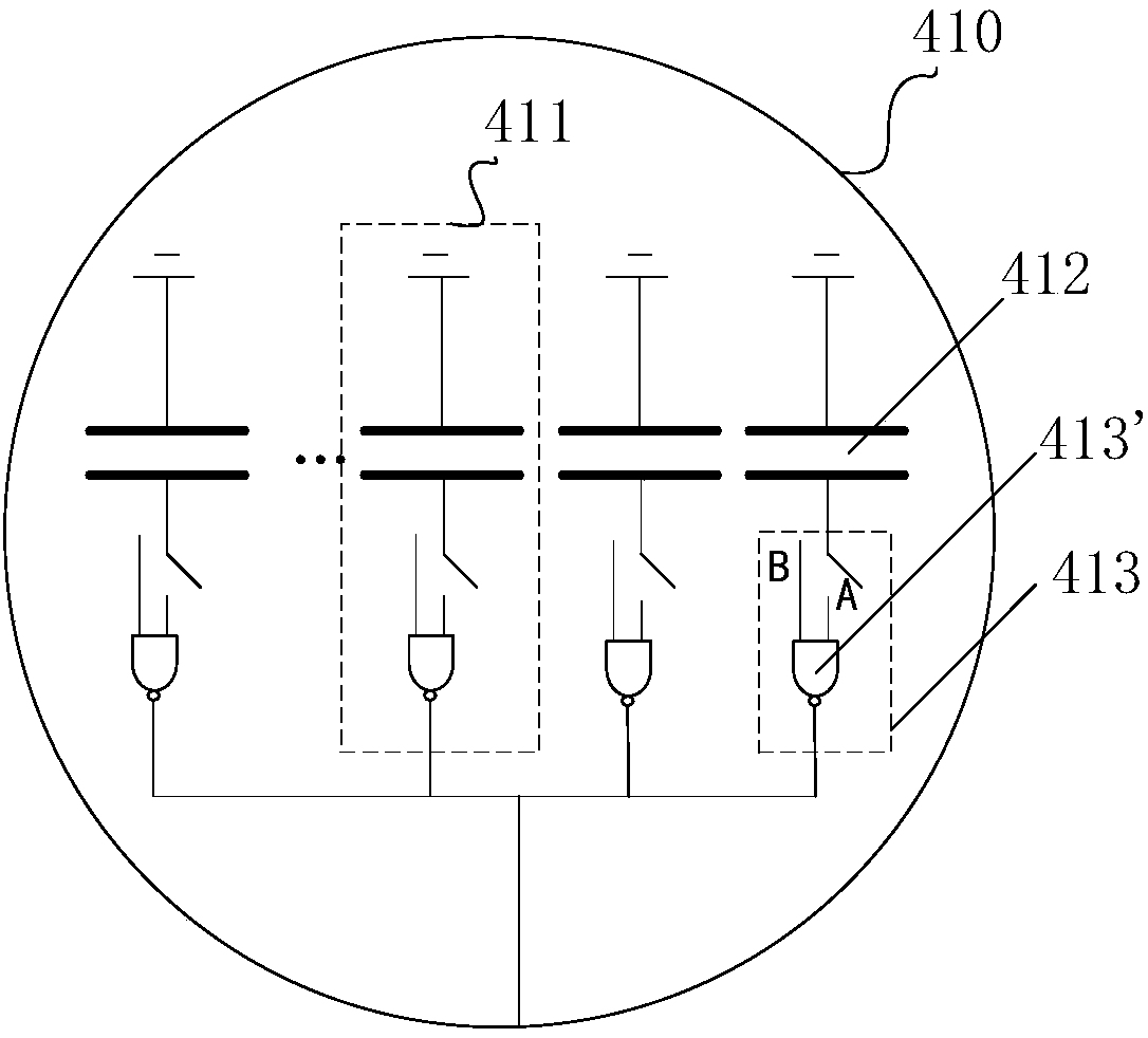
[0063] The first latch 100, the first buffer 600, the first buffer 600 is used to receive the first time pulse T IN1 The first latch input 111 of the first latch is connected to the output of the first buffer 600, and the second latch input 121 of the first latch receives the second time pulse T IN2 , the Q output terminal 112 of the first latch is coupled with a first capacitor 410, the first latch The output terminal 122 is coupled with a second capacitor 420;

[0064] The first D flip-flop 300, the first trigger input terminal 311 of the first D flip-flop receives from the first buffer 600 the first time pulse T delayed by a predetermined time interval IN1 , the second trigger input 312 of the first D flip-flop receives the second time pulse T IN2 , the first trigger output terminal 313 of the first D flip-flop is connected to at least one of the first capacitor 410 and the second capacitor ...

Embodiment 2

[0083] In another specific implementation manner, a semiconductor memory is also provided, including the time amplifier described in any one of the above.


PUM


Abstract

The invention provides a time amplifier. At least one D trigger is embedded in the time amplifier. If a time point when a first time pulse reaches a first D trigger after delay of a preset time interval is different from a time point when a second time pulse reaches the first D trigger, a logic signal output by the first D trigger controls and adjusts the capacitance value of a second capacitor tobe less than the capacitance value of a first capacitor, so that the amplification gains of the time amplifier are reduced; or a logic signal output by the first D trigger controls and adjusts the capacitance value of the first capacitor to be less than the capacitance value of the second capacitor, so that the amplification gains of the time amplifier are increased. Thus, the gains of the time amplifier are adjustable. The invention also provides a semiconductor memory which has the above-mentioned technical effects.

Description

technical field [0001] The invention relates to the technical field of semiconductors, in particular to a time amplifier and also to a semiconductor memory. Background technique [0002] Delay-locked loop (DLL, Delay-Locked Loop) is usually used in DDR3 / DDR4 dynamic random access memory. The delay-locked loop is used to automatically adjust the delay of one signal to make the phases of the two signals consistent (edge ​​alignment) . Specifically, when some digital signals need to be synchronized with the system clock, the delay-locked loop aligns the edges of the two clocks, and uses the adjusted clock as the control signal to generate a signal that is strictly synchronized with the system clock, and The synchronization does not change with changes in external conditions such as temperature and voltage, so it is widely used. [0003] In order to measure fine time intervals, a time-to-digital converter (TDC, Time-to-Digital converter) is embedded in the DLL. In recent years...

Claims


Application Information

Patent Timeline
Patent Type & Authority Applications(China)
IPC IPC(8): H03G3/30
CPCH03G3/30
Inventor 赖荣钦
Owner CHANGXIN MEMORY TECH INC
Why Eureka
Try Eureka