Pixel circuit and driving method thereof

A pixel circuit and electrical connection technology, applied in the display field, can solve the problems affecting the symmetry and matching state of other main devices, and increase the difficulty of the manufacturing process, so as to achieve the effect of improving the flickering degree of the screen, improving the stability, and increasing the holding ability

Active Publication Date: 2018-02-06
EVERDISPLAY OPTRONICS (SHANGHAI) CO LTD
View PDF11 Cites 23 Cited by
  • Summary
  • Abstract
  • Description
  • Claims
  • Application Information

AI Technical Summary

Problems solved by technology

But doing so will cause new problems: first, if the design rules are violated or the design is adjusted too much, it will affect the symmetry and matching state of other main devices; second, as the thickness of the interlayer capacitor dielectric decreases, the difficulty of the process will be enlarged, and new derivative problems will be generated on other related layers

Method used


Image

  • Pixel circuit and driving method thereof
  • Pixel circuit and driving method thereof
  • Pixel circuit and driving method thereof

Examples


Embodiment 1

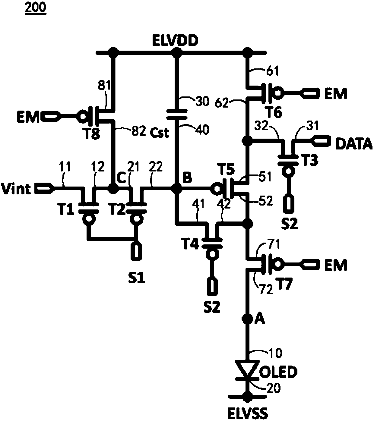
[0042] figure 2 is a schematic structural diagram of a pixel circuit according to Embodiment 1 of the present invention. According to this embodiment, the circuit 200 includes: a first transistor T1, whose first terminal 11 is connected to the input voltage Vint; a second transistor T2, whose first terminal 21 is electrically connected to the second terminal 12 of the first transistor T1, the first The control ends of the transistor T1 and the second transistor T2 are electrically connected to the first scan signal S1; the third transistor T3, the first end 31 of which is electrically connected to the data signal DATA; the fourth transistor T4, whose first end 41 is electrically connected to the second transistor The second terminal 22 of T2, the control terminals of the third transistor T3 and the fourth transistor T4 are electrically connected to the second scanning signal S2; the fifth transistor T5, the first terminal 51 of which is electrically connected to the second te...

Embodiment 2

[0055] Figure 4is a schematic structural diagram of a pixel circuit 400 according to Embodiment 2 of the present invention. The difference between the pixel circuit 400 of this embodiment and the pixel circuit 200 of the first embodiment is that it further includes a ninth transistor T9, the first terminal 91 of the ninth transistor T9 is electrically connected to the second terminal of the fourth transistor T4 42 and the second terminal 82 of the eighth transistor T8, the second terminal 92 thereof is electrically connected to the second terminal 52 of the fifth transistor T5, and the control terminal thereof is electrically connected to the second scanning signal S2.

[0056] Continue to refer to Figure 3 for the Figure 4 The timing diagram of the driving method of the pixel circuit shown, during the reset period, the first scan signal S1 is at low level, the second scan signal S2 and the control signal EM are at high level, at this time the first transistor T1 and the se...

Embodiment 3

[0060] Figure 5 is a schematic structural diagram of a pixel circuit 500 according to Embodiment 3 of the present invention. The pixel circuit 500 of this embodiment differs from the pixel circuit 200 of the first embodiment above in that it further includes a tenth transistor T10, the first terminal 101 of which is electrically connected to the second terminal 72 of the seventh transistor T7, and the second The terminal 102 is electrically connected to the input voltage Vint, and its control terminal is electrically connected to the third scanning signal S3. The tenth transistor T10 may be used to implement a reset function of a light emitting diode (eg, OLED).

[0061] refer to Image 6 for Figure 5 In the timing diagram of the driving method of the pixel circuit shown, a release period is added to the circuit due to the addition of the third scanning signal S3.

[0062] During the reset period, the first scanning signal S1 is at low level, the second scanning signal S...


PUM


Abstract

The disclosure relates to a pixel circuit and a driving method thereof. The pixel circuit comprises a first transistor and a second transistor whose control terminals receive first scanning signals; athird transistor and a fourth transistor whose control terminals receive second scanning signals; a fifth transistor whose control terminal is electrically connected to a first capacitor; a sixth transistor, a seventh transistor, and an eighth transistor whose control terminals receive control signals; and a light emitting diode. According to the pixel circuit and the driving method thereof, an electric leakage current can be reduced or reversely supplemented, the capacitance maintenance capability of the capacitor is improved, the flickering degree of images can be improved, and the stability of the displayed images is improved.

Description

technical field [0001] The present disclosure relates to the field of display technology, in particular, to a pixel circuit and a driving method thereof. Background technique [0002] Compared with the liquid crystal display panel in the traditional technology, the OLED (Organic Light Emitting Diode, Organic Light Emitting Diode) display panel has the characteristics of faster response speed, better color purity and brightness, higher contrast ratio, and wider viewing angle. Therefore, it has gradually received more and more attention from display technology developers. [0003] figure 1 It is a pixel circuit of an existing light-emitting display device. The pixel circuit includes: a first transistor T1, the control end of which is electrically connected to the first scanning signal S1, and the first end of the first transistor T1 is electrically connected to the input voltage Vint; the second transistor T2 and the third transistor T3, the control of both terminal is elec...

Claims


Application Information

Patent Timeline
Patent Type & Authority Applications(China)
IPC IPC(8): G09G3/3258G09G3/3266
CPCG09G3/3258G09G3/3266G09G3/3233G09G2300/0861G09G2310/0251G09G2310/0262G09G2320/0247
Inventor 郑士嵩
Owner EVERDISPLAY OPTRONICS (SHANGHAI) CO LTD
Why Eureka
Try Eureka