Method for manufacturing circuit board

A production method and circuit board technology, which is applied in the fields of printed circuit manufacturing, printed circuit, electrical components, etc., can solve problems such as inability to meet special surface copper requirements, lack of special functions of circuit boards, and inability to meet customer requirements for solder-resisting plug holes.

Inactive Publication Date: 2018-02-06
深圳明阳电路科技股份有限公司
View PDF4 Cites 1 Cited by
  • Summary
  • Abstract
  • Description
  • Claims
  • Application Information

AI Technical Summary

Problems solved by technology

[0003] With the rapid development of informatization, electronic products are developing towards diversified functions and portable functions. Fine lines, micro-holes and high density have become common phenomena, and some printed circuit boards with special structures have appeared. For example, customers require some high-frequency The copper thickness of the finished product in the local area of ​​the board is required to be Hoz, and the copper thickness of the finished product in the local area is required to be 1oz. The thickness of the bottom copper has b

Method used


Image

  • Method for manufacturing circuit board

Examples


Embodiment Construction

[0016] It should be noted that, in the case of no conflict, the embodiments in the present application and the features in the embodiments can be combined with each other.

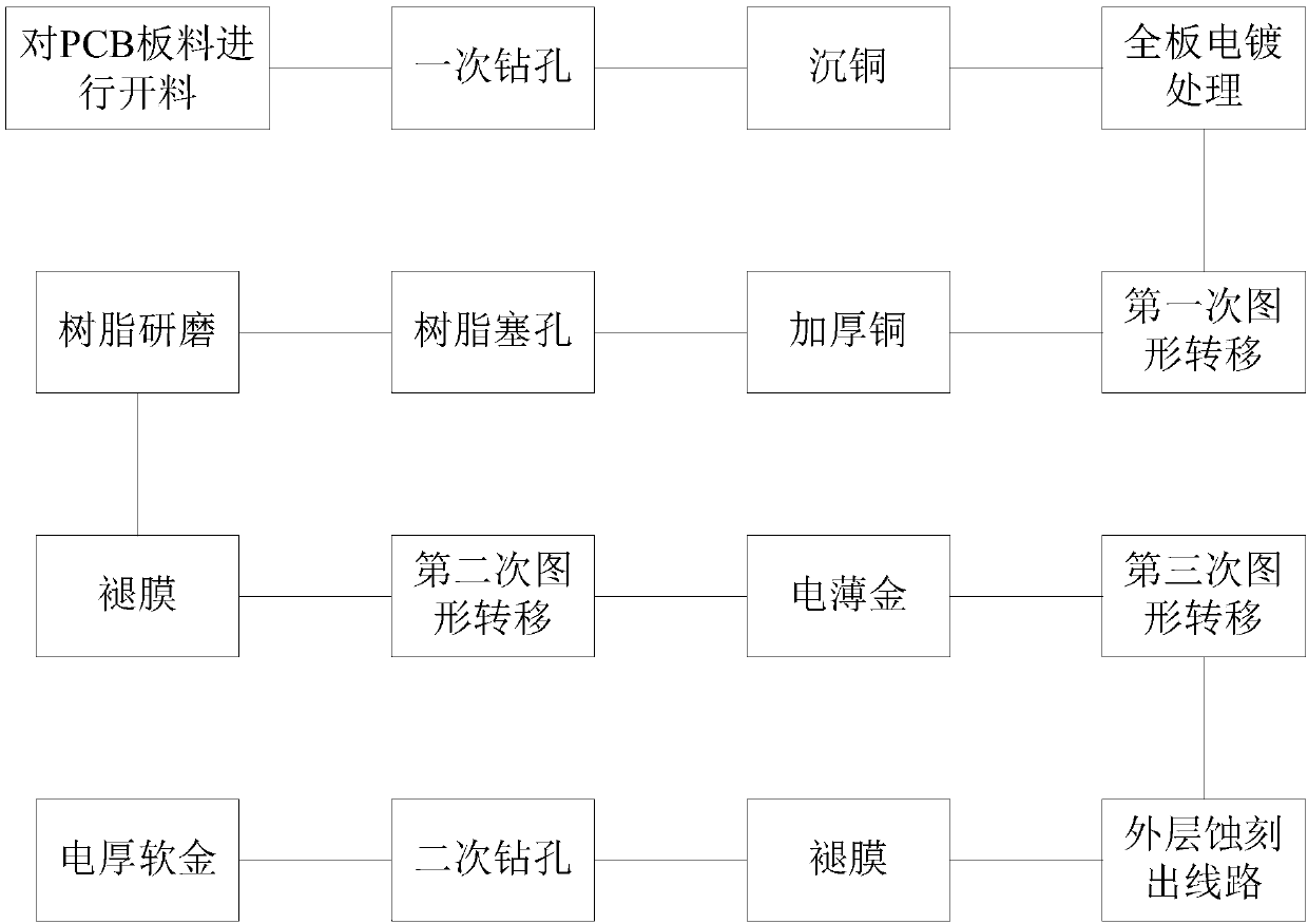
[0017] Such as figure 1 Shown, a kind of manufacturing method of circuit board, it comprises the following steps: Carry out material cutting to PCB board material, one-time drilling, sinking copper, whole board electroplating treatment, first pattern transfer, thicken copper, resin plug hole, Resin grinding, film stripping, second pattern transfer, electro-thin gold, third pattern transfer, electro-thick soft gold, secondary drilling, film stripping, outer layer etching of circuits and subsequent process production.

[0018] The specific implementation of each step is described below:

[0019] Primary drilling and secondary drilling: Drill PTH holes (sinking copper holes) and NPTH holes (non-sinking copper holes) respectively.

[0020] Among them, when the resin is plugged, the whole board vacuum pluggin...


PUM


Abstract

The invention discloses a method for manufacturing a circuit board. The method comprises the following steps: carrying out rough shape cutting on a PCB material; carrying out primary hole drilling; carrying out plated-through-hole processing; carrying out whole-board electroplating processing; carrying out first-time pattern transferring, carrying out copper thickening; carrying out resin hole plugging; carrying out resin grinding; carrying out film removing; carrying out second-time pattern transferring; carrying out flash gold processing; carrying out third-time pattern transferring; carrying out electric thick soft gold processing; carrying out secondary hole drilling; carrying out film removing; and carrying out outer-layer line etching. According to the invention, selective electroplating is carried out by two-times line transferring, so that the local copper thickness request is met. With the resin hole plugging and the third-time pattern transferring, requirements of plugged hole evenness and fullness from the client are met; and the line is bound with the PAD electric thick soft gold partially, so that application of the special function is realized.

Description

technical field [0001] The invention relates to the technical field of circuit board production, in particular to a method for manufacturing a circuit board. Background technique [0002] CS often represents the front (Top) side of the outermost layer, and the reverse side of the outermost layer is generally represented by SS. [0003] With the rapid development of informatization, electronic products are developing towards diversified functions and portable functions. Fine lines, micro-holes and high density have become common phenomena, and some printed circuit boards with special structures have appeared. For example, customers require some high-frequency The copper thickness of the finished product in the local area of ​​the board is required to be Hoz, and the copper thickness of the finished product in the local area is required to be 1oz. The thickness of the bottom copper has both Hoz and 1oz; The degree of hole is flat and full; the surface treatment requirement is...

Claims


Application Information

Patent Timeline
IPC IPC(8): H05K3/02H05K3/42
CPCH05K3/02H05K3/423H05K2203/0723
Inventor 张永辉孙启双
Owner 深圳明阳电路科技股份有限公司
Why Eureka
Try Eureka