OLED touch display substrate, manufacturing method, display panel and display apparatus

A touch display substrate and touch electrode technology, which is applied in the fields of instruments, electrical digital data processing, electrical components, etc., can solve problems such as being unsuitable for products with large sizes, and achieve low cost, realization of conduction, and simple manufacturing process. Effect

Active Publication Date: 2018-02-16
BOE TECH GRP CO LTD
View PDF17 Cites 39 Cited by
  • Summary
  • Abstract
  • Description
  • Claims
  • Application Information

AI Technical Summary

Problems solved by technology

This structure is achievable for small-sized embedded self-capacitance touch screen products, but with the increase of touch electrode blocks, the surrounding wiring area will form a touch blind area, and the large width of the touch blind area is directly controlled by the touch panel. The number of sensors is determined, so this structure is not suitable for larger products

Method used


Image

  • OLED touch display substrate, manufacturing method, display panel and display apparatus
  • OLED touch display substrate, manufacturing method, display panel and display apparatus
  • OLED touch display substrate, manufacturing method, display panel and display apparatus

Examples


Embodiment Construction

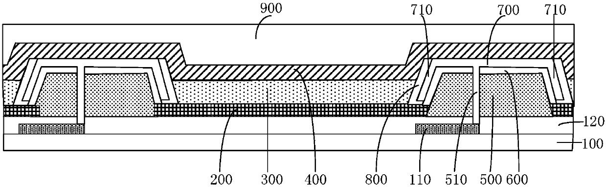
[0037] In order to illustrate the present invention more clearly, the present invention will be further described in detail below in conjunction with preferred embodiments and accompanying drawings. In the following detailed description, numerous specific details are set forth in order to provide a thorough understanding of the embodiments of the present disclosure. However, one skilled in the art would understand that one or more embodiments may be practiced without the specific details. In other instances, well-known structures and devices are shown in diagrammatic form to simplify the drawings. It should be noted that the word "comprising" does not exclude other elements or steps, and the word "a" or "an" does not exclude a plurality. In addition, the expression "on" used in the specification may mean that one component is disposed directly above another component, or that one component is disposed above another component, and there is an intermediate layer between the two...


PUM


Abstract

The invention discloses an OLED touch display substrate, a manufacturing method for the substrate, a display panel and a display apparatus. The OLED touch display substrate comprises a positive electrode and a negative electrode located on a substrate, an organic luminous layer located between the positive electrode and the negative electrode, and a pixel definition layer provided with via holes;the negative electrode comprises multiple sub-negative electrodes insulated mutually; the sub-negative electrodes are multiplexed as touch electrodes; and the OLED touch display substrate further comprises touch signal lines electrically connected with the touch electrodes through the via holes in a one-to-one correspondence manner. The OLED touch display substrate is small in thickness and free of a touch blind area.

Description

technical field [0001] The invention relates to the technical field of touch display. More specifically, it relates to an OLED touch display substrate, a manufacturing method, a display panel and a display device. Background technique [0002] Organic Light Emitting Diode (OLED) is one of the hotspots in the field of flat panel display research. Compared with liquid crystal displays, OLED has the advantages of low energy consumption, self-illumination, wide viewing angle, fast response speed, and low production cost, so it has gradually replaced traditional LCD displays in the display fields of mobile phones, PDAs, and digital cameras. Among them, the design of pixel driving circuit is the core technical content of OLED display, which has important research significance. [0003] At present, most of the existing OLED-based touch products adopt the plug-in touch structure, that is, the touch panel is combined with the TFE packaging structure of the OLED display substrate to...

Claims


Application Information

Patent Timeline
Patent Type & Authority Applications(China)
IPC IPC(8): G06F3/041G06F3/044H01L27/32
CPCG06F3/0412G06F3/044H10K59/40H10K59/131H10K59/1201
Inventor 杨盛际董学陈小川玄明花王磊卢鹏程王治肖丽刘冬妮
Owner BOE TECH GRP CO LTD
Why Eureka
Try Eureka