Display panel and display device

A display panel and substrate technology, which is applied in the direction of identification devices, instruments, electrical components, etc., can solve problems such as abnormal display of the display panel, short circuit between the anode film layer and the source-drain layer, and failure of the drive circuit to work normally. Normal work, the effect of improving adhesion

Inactive Publication Date: 2018-02-16
WUHAN CHINA STAR OPTOELECTRONICS SEMICON DISPLAY TECH CO LTD
View PDF3 Cites 4 Cited by
  • Summary
  • Abstract
  • Description
  • Claims
  • Application Information

AI Technical Summary

Problems solved by technology

[0003] The technical problem existing in the packaging structure of the existing flexible display panel is: it is easy to cause the anode film layer to pierce the lower organic film layer in the subsequent packaging process, and then the anode film layer is short-circuited with the source and drain layers, causing the drive circuit to fail to work normally. The entire display panel is displayed abnormally

Method used


Image

  • Display panel and display device

Examples


Embodiment Construction

[0021] The technical solutions in the embodiments of the present invention will be clearly and completely described below in conjunction with the accompanying drawings in the embodiments of the present invention. Obviously, the described embodiments are only a part of the embodiments of the present invention, rather than all the embodiments. Based on the embodiments of the present invention, all other embodiments obtained by those of ordinary skill in the art without creative work shall fall within the protection scope of the present invention.

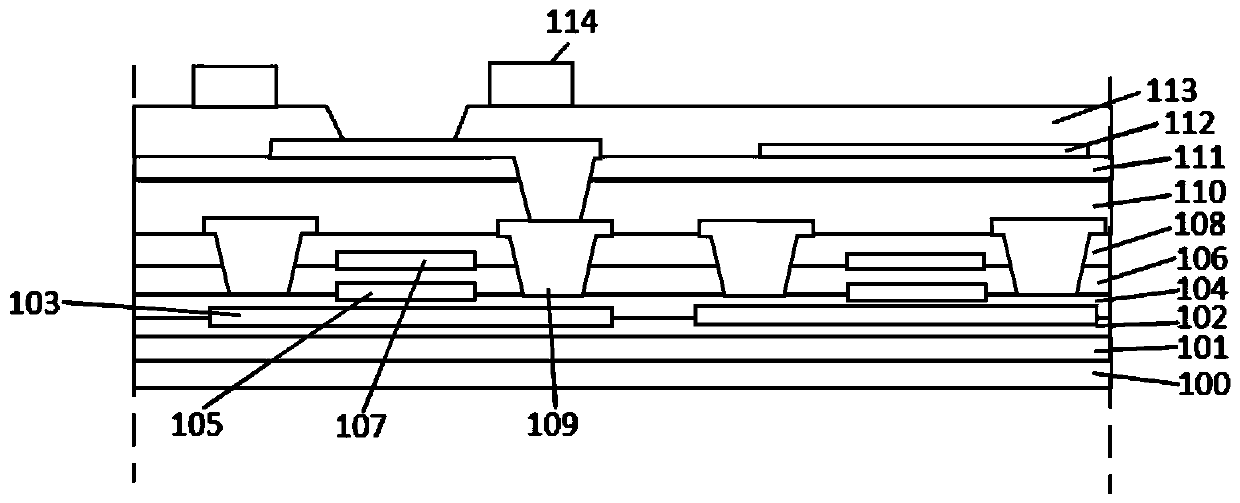
[0022] Such as figure 1 Shown is the first embodiment of the display panel structure of the present invention.

[0023] The display panel in this embodiment includes: a substrate 100; a substrate thin film layer 101 disposed on the substrate 100; a flat layer 110 disposed on the substrate thin film layer 101, a functional layer sequentially formed on the flat layer 110, and a functional layer structure It includes at least: an anode film ...


PUM


Abstract

The invention discloses a display panel comprising a substrate thin film layer, an organic thin film layer disposed on the substrate thin film layer, a flat layer disposed on the organic thin film layer, and functional layers sequentially formed on the flat layer. The functional layers consist at least of an anode film layer. An inorganic insulating film layer is further arranged between the anodefilm layer and a pattern of the flat layer, and the inorganic insulating film layer is consistent with the pattern of the flat layer. The invention also discloses a display device. The display paneland the display device in the invention can be used to prevent the anode film layer from puncturing the organic thin film layer below, improve the adhesion between the anode film layer and the underlying film layer and ensure the normal driving of the circuit outside a display area and the normal image display.

Description

Technical field [0001] The present invention relates to the field of display panel manufacturing, in particular to a display panel and a display device. Background technique [0002] Flexible display technology is the next-generation mainstream display technology. In the prior art, flexible display panels are mainly driven by active matrix low-temperature polysilicon thin film transistors. In the manufacturing process, in order to ensure the adhesion of the anode film of the display panel, it is necessary to make equidistant circles or circles on the anode film outside the display area. Square hole. [0003] The existing technical problem of the packaging structure of the flexible display panel is that it is easy to cause the anode film layer to pierce the underlying organic film layer in the subsequent packaging process, and then the anode film layer and the source and drain layer are shorted, causing the driving circuit to fail to work normally. The entire display panel screen ...

Claims


Application Information

Patent Timeline
Patent Type & Authority Applications(China)
IPC IPC(8): H01L27/12H01L51/50H01L51/56G09F9/30
CPCH01L27/1214H01L27/1222H01L27/1259G09F9/301H10K50/00H10K71/00
Inventor 王幸
Owner WUHAN CHINA STAR OPTOELECTRONICS SEMICON DISPLAY TECH CO LTD
Why Eureka
Try Eureka