memory device

A storage device, free technology, applied in fields such as magnetic field-controlled resistors, components of electromagnetic equipment, material selection, etc., can solve the problems of difficulty in manufacturing memory, high energy of free layer rotation, and difficulty in storage manufacturing.

Active Publication Date: 2021-01-12
IUCF HYU (IND UNIV COOP FOUNDATION HANYANG UNIV)
View PDF4 Cites 0 Cited by
  • Summary
  • Abstract
  • Description
  • Claims
  • Application Information

AI Technical Summary

Problems solved by technology

However, using conventional SiO 2 or MgO to make the magnetic tunnel junction, when considering the connection with the actual triode, it is difficult to directly store and manufacture
[0006] Moreover, in order to realize the spin

Method used


Image

  • memory device
  • memory device
  • memory device

Examples


Embodiment Construction

[0034] Hereinafter, embodiments of the present invention will be described in detail with reference to the drawings. However, the present invention is not limited to the embodiments disclosed below, and can be embodied in various forms, but this embodiment makes the disclosure of the present invention complete, and provides the present invention to those of ordinary skill in the technical field of the present invention. category.

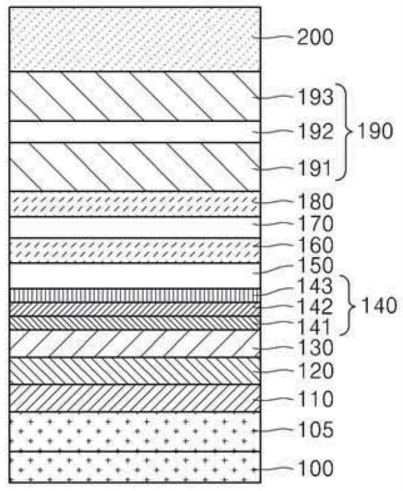
[0035] figure 1 It is a cross-sectional view of a storage device according to an embodiment of the present invention, a cross-sectional view of a spin-torque magnetic random access memory device.

[0036] refer to figure 1 The storage device according to an embodiment of the present invention includes a lower electrode 110 formed on a substrate 100, a buffer layer 120, a seed layer 130, a free layer 140, a magnetic tunnel barrier 150, a pinned layer 160, a cover layer 170, a second buffer layer 180, And synthesize the exchange semimagnetic layer ...


PUM

PropertyMeasurementUnit
Thicknessaaaaaaaaaa
Thicknessaaaaaaaaaa
Thicknessaaaaaaaaaa

Abstract

Disclosed is a memory device having a magnetic tunnel junction comprising a free layer, a tunnel barrier and a pinned layer, wherein the free layer comprises at least two layers having magnetism of mutually different directions.

Description

technical field [0001] The present invention relates to a memory device, and in particular, to a magnetic memory device utilizing a magnetic tunnel junction (Magnetic Tunnel Junction, MTJ). Background technique [0002] Conduct research on next-generation nonvolatile memory devices that consume less power and have higher set precision than flash memory devices. Such next-generation nonvolatile memory devices include phase change RAM (PRAM) utilizing state changes of phase change substances such as chalcogenide alloys, magnetic tunnels utilizing ferromagnetism-based magnetization states, The magnetic memory (MagneticRAM, MRAM) that uses the impedance change of the junction (Magnetic Tunnel Junction, MTJ), the ferroelectric memory (Ferroelectric RAM) that uses the hierarchical phenomenon of ferroelectric materials, and the resistance change memory that uses the impedance change of the variable impedance material (Resistance change RAM, ReRAM), etc. [0003] As a magnetic mem...

Claims


Application Information

Patent Timeline
IPC IPC(8): H01L43/02H01L43/10H01L43/08
Inventor 朴在勤李承垠
Owner IUCF HYU (IND UNIV COOP FOUNDATION HANYANG UNIV)
Why Eureka
Try Eureka