Back-illuminated imaging sensor packaging structure and preparing method thereof
An image sensor and packaging structure technology, which is applied to electric solid state devices, semiconductor devices, radiation control devices, etc., can solve the problems of cumbersome and complicated process steps and high cost, and achieve the effects of shortening process time, saving costs, and saving process steps.
- Summary
- Abstract
- Description
- Claims
- Application Information
AI Technical Summary
Problems solved by technology
Method used
Image

Examples
Embodiment 1
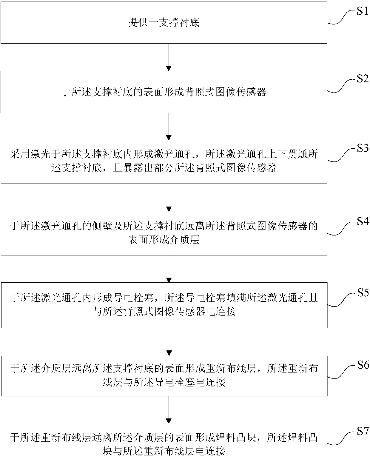
[0064] see figure 1 , the present embodiment provides a method for preparing a package structure of a back-illuminated image sensor, the method for preparing a package structure of a back-illuminated image sensor includes the following steps:
[0065] 1) providing a supporting substrate;
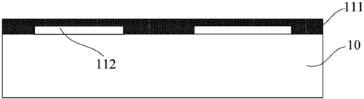
[0066] 2) forming a back-illuminated image sensor on the surface of the supporting substrate;
[0067] 3) using a laser to form a laser through hole in the support substrate, the laser through hole penetrates the support substrate up and down, and exposes part of the back-illuminated image sensor;
[0068]4) forming a dielectric layer on the sidewall of the laser through hole and the surface of the support substrate away from the back-illuminated image sensor;
[0069] 5) forming a conductive plug in the laser through hole, the conductive plug filling the laser through hole and electrically connecting with the back-illuminated image sensor;
[0070] 6) forming a rewiring layer on the surf...
Embodiment 2
[0107] read on Figure 14, this embodiment also provides a back-illuminated image sensor packaging structure, the back-illuminated image sensor packaging structure can be prepared by using, but not limited to, the preparation method of the back-illuminated image sensor packaging structure described in Embodiment 1 , the back-illuminated image sensor packaging structure includes: a support substrate 10; a back-illuminated image sensor 11, the back-illuminated image sensor 11 is located on the support substrate 10; a laser through hole 12, the laser through The hole 12 is located in the support substrate 10, and penetrates the support substrate 10 up and down to expose part of the back-illuminated image sensor 11; a dielectric layer 13, the dielectric layer 13 is located in the laser through hole 12 The sidewall of the support substrate 10 and the surface away from the back-illuminated image sensor 11; the conductive plug 14, the conductive plug 14 is located in the laser throug...
PUM
 Abstract
Description
Claims
Application Information
 - Generate Ideas
- Intellectual Property
- Life Sciences
- Materials
- Tech Scout
- Unparalleled Data Quality
- Higher Quality Content
- 60% Fewer Hallucinations
Browse by: Latest US Patents, China's latest patents, Technical Efficacy Thesaurus, Application Domain, Technology Topic, Popular Technical Reports.
© 2025 PatSnap. All rights reserved.Legal|Privacy policy|Modern Slavery Act Transparency Statement|Sitemap|About US| Contact US: help@patsnap.com