Preparation method for low-temperature film transistor
A thin-film transistor, low-temperature technology, used in semiconductor/solid-state device manufacturing, semiconductor devices, electrical components, etc., can solve problems such as low storage capacity and toxicity, and achieve improved uniformity, improved interface quality, and reduced sub-threshold swing. Effect
- Summary
- Abstract
- Description
- Claims
- Application Information
AI Technical Summary
Problems solved by technology
Method used
Image

Examples
Embodiment 1
[0032] Preparation:
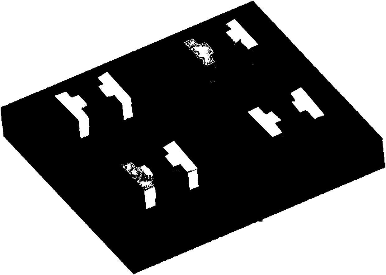
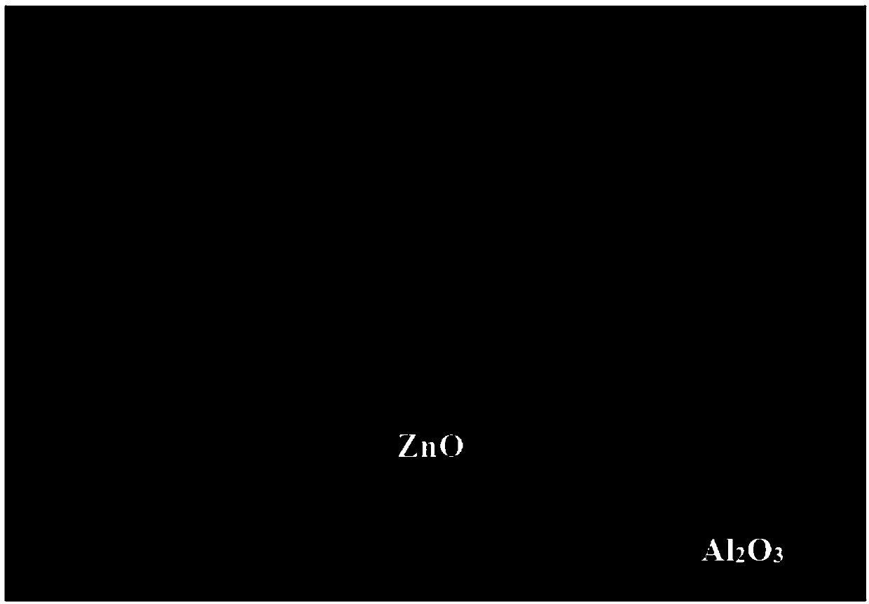
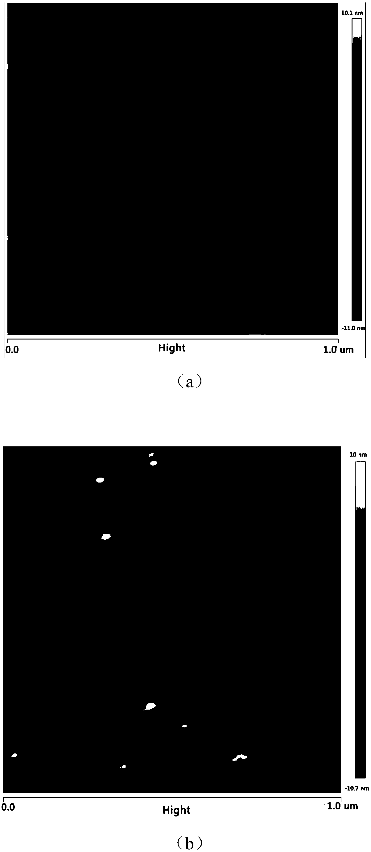
[0033] like figure 1 and 2 As shown, the heavily doped P-type Si substrate was placed in an ALD reaction chamber, and Al was deposited at 80 °C. 2 O 3 Gate insulating layer 36nm; using in-situ growth method, at 80 ℃, directly on Al 2 O 3 Deposit ZnO on 15nm. The obtained device is processed in the ultra-clean room, and the first photolithography is performed first. The processing conditions are: use positive glue, use a glue homogenizer, first use 600r / s, turn for 9s, and then use 4000r / s, turn for 1min. After baking at 115°C for 1 min, use an exposure machine to expose for 14 s. Afterwards, a positive film developer was used for 20s development. Next, the channel is etched, and after being etched in phosphoric acid for 25s, the residual phosphoric acid is washed in deionized water. Then use acetone to remove the glue. Then carry out secondary photolithography, negative glue, use a glue dispenser, first use 600r / s, turn for 9s, then use 4000r / s, tu...
Embodiment 2
[0037] Preparation:
[0038] Put the ITO / PET substrate into the ALD reaction chamber and deposit Al at 80°C 2 O 3 Gate insulating layer 36nm; using in-situ growth method, at 100 ℃, directly on Al 2 O 3 Deposit ZnO 20nm on it. The obtained device is processed in the ultra-clean room, and the first photolithography is performed first. The processing conditions are: use positive glue, use a glue homogenizer, first use 600r / s, turn for 9s, and then use 4000r / s, turn for 1min. After baking at 115°C for 1 min, use an exposure machine to expose for 14 s. Afterwards, a positive film developer was used for 20s development. Next, the channel is etched, and after being etched in phosphoric acid for 25s, the residual phosphoric acid is washed in deionized water. Then use acetone to remove the glue. Then carry out secondary photolithography, negative glue, use a glue dispenser, first use 600r / s, turn for 9s, then use 4000r / s, turn for 1min. After pre-baking at 90 °C for 1 min, use ...
Embodiment 3
[0042] Preparation:
[0043] Put the heavily doped P-type Si substrate into the ALD reaction chamber and deposit Al at 100 °C 2 O 3 Gate insulating layer 36nm; using in-situ growth method, at 100 ℃, directly on Al 2 O 3 Deposit ZnO on 15nm. The obtained device is processed in the ultra-clean room, and the first photolithography is performed first. The processing conditions are: use positive glue, use a glue homogenizer, first use 600r / s, turn for 9s, and then use 4000r / s, turn for 1min. After baking at 115°C for 1 min, use an exposure machine to expose for 14 s. Afterwards, a positive film developer was used for 20s development. Next, the channel is etched, and after being etched in phosphoric acid for 25s, the residual phosphoric acid is washed in deionized water. Then use acetone to remove the glue. Then carry out secondary photolithography, negative glue, use a glue dispenser, first use 600r / s, turn for 9s, then use 4000r / s, turn for 1min. After pre-baking at 90 °C ...
PUM
 Abstract
Description
Claims
Application Information
 - R&D Engineer
- R&D Manager
- IP Professional
- Industry Leading Data Capabilities
- Powerful AI technology
- Patent DNA Extraction
Browse by: Latest US Patents, China's latest patents, Technical Efficacy Thesaurus, Application Domain, Technology Topic.
© 2024 PatSnap. All rights reserved.Legal|Privacy policy|Modern Slavery Act Transparency Statement|Sitemap