A packaging structure and method for a non-electrically connected chip

A technology of electrical connection and packaging structure, which is applied in the direction of electrical components, electrical components to assemble printed circuits, circuits, etc., to achieve the effects of increasing the scope of application scenarios, improving performance, and reducing burdens

Active Publication Date: 2020-03-17
FUZHOU ROCKCHIP SEMICON
View PDF6 Cites 0 Cited by
  • Summary
  • Abstract
  • Description
  • Claims
  • Application Information

AI Technical Summary

Problems solved by technology

[0004] The technical problem to be solved by the present invention is to provide a chip packaging structure and packaging method. The whole chip does not have any external physical and electrical connection interface, and a single chip can work independently without an external printed circuit board. Charging and charging can be completed wirelessly. Communication can make the chip work in the environment where the original electronic equipment can't work in the middle of the water and the human body, which greatly improves the scope of application scenarios of the Internet of Things chip

Method used


Image

  • A packaging structure and method for a non-electrically connected chip
  • A packaging structure and method for a non-electrically connected chip
  • A packaging structure and method for a non-electrically connected chip

Examples


Embodiment Construction

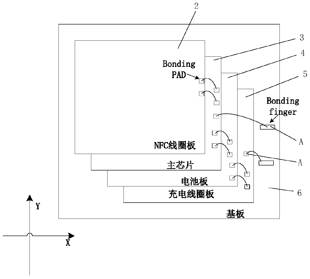
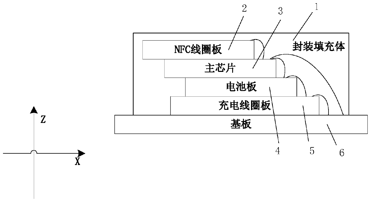
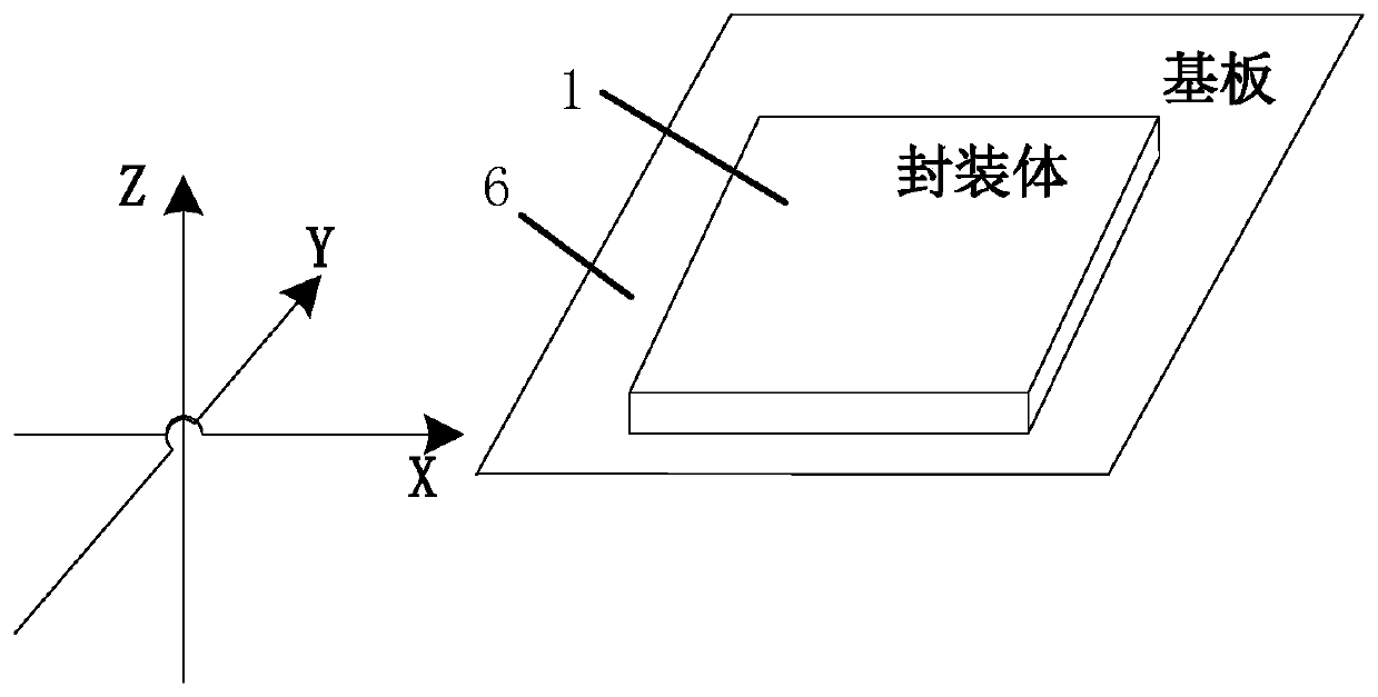
[0039] see Figure 1 to Figure 3 As shown, the chip packaging structure of the present invention includes a fully enclosed injection molded body 1 and an NFC coil film or board 2, a main chip 3, a battery board 4, a wireless charging coil film or board 5 or plate and substrate 6;

[0040] Between the NFC coil film 2 or board and the main chip 3, between the main chip 3 and the battery board 4, between the battery board 4 and the wireless charging coil film or board 5, and the wireless charging coil film or board 5 and the substrate 6, and between the main chip 3 and the substrate 6 are respectively welded by welding wires; the main chip 3 is welded to the NFC coil film or plate 5 by two welding wires respectively, and connected to The battery board 4 is welded, and welded to the substrate 3 through at least one welding wire; the wireless charging coil film or plate 5 is welded to the battery board 4 through two welding wires, and connected to the battery board 4 through one w...


PUM


Abstract

The invention provides a packaging structure for chips without electrical connection, including a fully enclosed injection molded body, an NFC coil film or board, a main chip, a battery board, a wireless charging coil film or board, and a substrate that are stacked and fixed sequentially from top to bottom between the NFC coil film or plate and the main chip, between the main chip and the battery plate, between the battery plate and the wireless charging coil film or plate, between the wireless charging coil film or plate and the substrate, and The main chip and the substrate are respectively welded by welding wires; the welded product is injection molded to form the fully enclosed injection molding body, and the upper surface of the fully enclosed injection molding body and the substrate is connected to the NFC coil film or board, the main chip, the battery, etc. The board, wireless charging coil film or board is wrapped inside, leaving no electrical interface on the surface. The whole chip of the present invention does not have any external physical electrical connection interface, which can make the chip work in a harsh environment and greatly improve the scope of application scenarios of the Internet of Things chip.

Description

technical field [0001] The invention relates to a chip package, in particular to a fully enclosed package method and structure of an Internet of Things chip. Background technique [0002] With the rapid development of SOC chip technology, the Internet of Things technology is becoming more and more important and the demand is increasing. However, an important problem currently restricting IoT chips is that all devices and basic chips still rely on traditional physical electrical devices, such as power sockets, debugging sockets, etc., for connection, information exchange and power charging, etc., so the devices cannot work. with harsh liquids or other harsh environments. [0003] After retrieval, most of the current research on chip packaging technology is to improve the performance of the chip, and there are few studies on the packaging technology of the chip in order to adapt to the working environment. Therefore, the present invention proposes a chip packaging design meth...

Claims


Application Information

Patent Timeline
Patent Type & Authority Patents(China)
IPC IPC(8): H01L23/31H01L25/00H05K3/34
CPCH01L25/00H05K3/34H05K3/3431H01L23/3107H01L23/3121H01L2924/181H01L2224/48091H01L2224/48145H01L2224/48227H01L2924/00014H01L2924/00012
Inventor 廖裕民
Owner FUZHOU ROCKCHIP SEMICON
Why Eureka
Try Eureka