
TFT assembly of curved liquid crystal display panel

A technology for liquid crystal display panels and components, applied in transistors, electrical components, semiconductor devices, etc., can solve problems such as dislocation and poor display of upper and lower substrates, and achieve the effect of improving optical performance

Inactive Publication Date: 2018-03-09
长沙惠科金扬科技有限责任公司
View PDF5 Cites 1 Cited by
  • Summary
  • Abstract
  • Description
  • Claims
  • Application Information

AI Technical Summary

Problems solved by technology

[0003] Curved liquid crystal display panels have a better viewing experience than traditional flat display panels, but curved liquid crystal display panels are prone to misalignment of the upper and lower substrates after bending, resulting in poor display

Method used


Image

  • TFT assembly of curved liquid crystal display panel

Examples


Embodiment 1

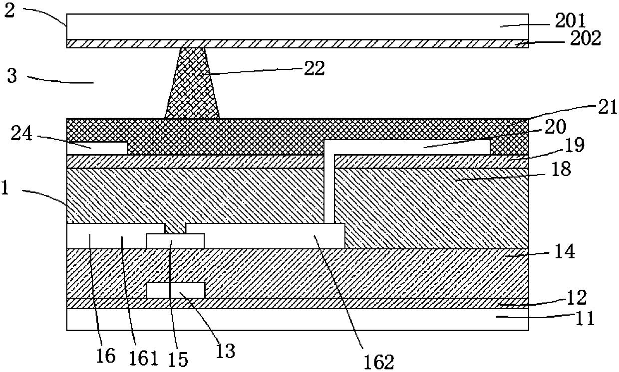
[0029] see figure 1 , the present invention provides a curved liquid crystal display panel, comprising: a first substrate 1 and a second substrate 2 arranged oppositely, and a liquid crystal layer 3 arranged between the first substrate 1 and the second substrate 2;

[0030] The first substrate 1 includes: a first base substrate 11, a plurality of scanning lines (not shown) formed on a side of the first base substrate 11 facing the second substrate 2, and a plurality of scanning lines perpendicular to the scanning lines. A data line 16, and a plurality of TFTs, covering the scanning line, the data line 16, and the insulating layer 18 of the TFT, the color resistance layer 19 disposed on the insulating layer 18, the color resistance layer 19 disposed on the color resistance layer 19 The pixel electrode 20 and the light-shielding electrode 24, the organic flat layer 21 covering the color resist layer 19, the pixel electrode 20, the light-shielding electrode 24, and the main gap s...

Embodiment 2

[0038] A method for processing a TFT component of a curved liquid crystal display panel, the steps are as follows:

[0039] 1), structure and separate processing

[0040] TFT components, including a gate on the buffer layer, a gate insulating layer covering the gate and the buffer layer, an active layer on the gate insulating layer, and an active layer on the gate insulating layer respectively The source and drain of both ends of the contact;

[0041] Each component is first prepared, assembled and compounded according to the existing technology;

[0042] 2), pre-processing

[0043] After compounding, spray the pretreatment liquid on the outer surface, and dry it with a vacuum dryer at the drying temperature of 35°C after spraying;

[0044] The components of the pretreatment liquid are: 3.5 parts of phthalates, 2.3 parts of anti-precipitation agent, 3.5 parts of leveling agent, 17 parts of glacial acetic acid, 25 parts of polystyrene resin, 2.5 parts of isatin base;

[004...


PUM


Abstract

The invention relates to the technical field of display, in particular to a TFT assembly of a curved liquid crystal display panel. The TFT assembly includes a grid electrode disposed on a buffer layer, a grid electrode insulating layer covering the grid electrode and the buffer layer, an active layer disposed on the grid electrode insulating layer, and a source electrode and a drain electrode which are disposed on the grid electrode insulating layer and are in contact with the two ends of the active layer. According to the TFT assembly of the curved liquid crystal display panel and a processing method thereof, the optical performance of the TFT assembly is significantly improved by pre-processing and subsequent processing.

Description

technical field [0001] The invention relates to the field of display technology, in particular to a TFT component of a curved liquid crystal display panel. Background technique [0002] Liquid Crystal Display (LCD) is widely used in mobile phones, TVs, personal digital assistants, digital cameras, notebook computers, desktop computers due to its advantages of high image quality, power saving, thin body and wide application range. Various consumer electronic products, such as LED display devices, have become the mainstream of display devices. [0003] Compared with the traditional flat display panel, the curved liquid crystal display panel has a better viewing experience, but the upper and lower substrates of the curved liquid crystal display panel are prone to misalignment after bending, resulting in poor display. Contents of the invention [0004] The technical problem to be solved by the present invention is to provide a curved liquid crystal display panel, which can pr...

Claims


Application Information

Patent Timeline
Patent Type & Authority Applications(China)
IPC IPC(8): G02F1/1368G02F1/1362G02F1/1343G02F1/1339G02F1/1333H01L29/786H01L21/336
CPCG02F1/1333G02F1/13394G02F1/13439G02F1/1362G02F1/1368G02F1/133357G02F1/13396G02F1/136218G02F1/136222H01L29/66742H01L29/786
Inventor 白航空
Owner 长沙惠科金扬科技有限责任公司
Learn More