Heating chamber and semiconductor processing device

A technology for heating chambers and chambers, which is applied in semiconductor/solid-state device manufacturing, electrical components, circuits, etc. It can solve problems such as product yield decline, large difference in gas flow rate, and poor process uniformity, so as to improve uniformity, gas flow rate, etc. The flow rate and flow rate are consistent, and the effect of improving product yield

Active Publication Date: 2018-03-09
BEIJING NAURA MICROELECTRONICS EQUIP CO LTD
View PDF8 Cites 4 Cited by
  • Summary
  • Abstract
  • Description
  • Claims
  • Application Information

AI Technical Summary

Problems solved by technology

[0004] Because the air outlets of the current air inlet mechanism are located at the edge of the heating chamber, this makes the distance between each air outlet and the edge of the wafer placed on the susceptor smaller than the distance between the center of the wafer, resulting in the flow through The gas flow rate and flow rate at the edge of the wafer are quite different from the gas flow rate flowing through the center of the wafer, resulting in the degree of carryover and dilution of the deposits at the edge of the wafer and the degree of carryover and dilution of deposits at the center of the wafer. Large differences, which in turn lead to poor process uniformity, resulting in a decline in product yield

Method used


Image

  • Heating chamber and semiconductor processing device
  • Heating chamber and semiconductor processing device
  • Heating chamber and semiconductor processing device

Examples


Embodiment Construction

[0014] In order for those skilled in the art to better understand the technical solution of the present invention, the heating chamber and semiconductor processing equipment provided by the present invention will be described in detail below with reference to the accompanying drawings.

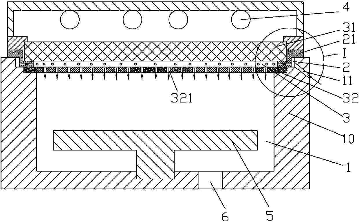
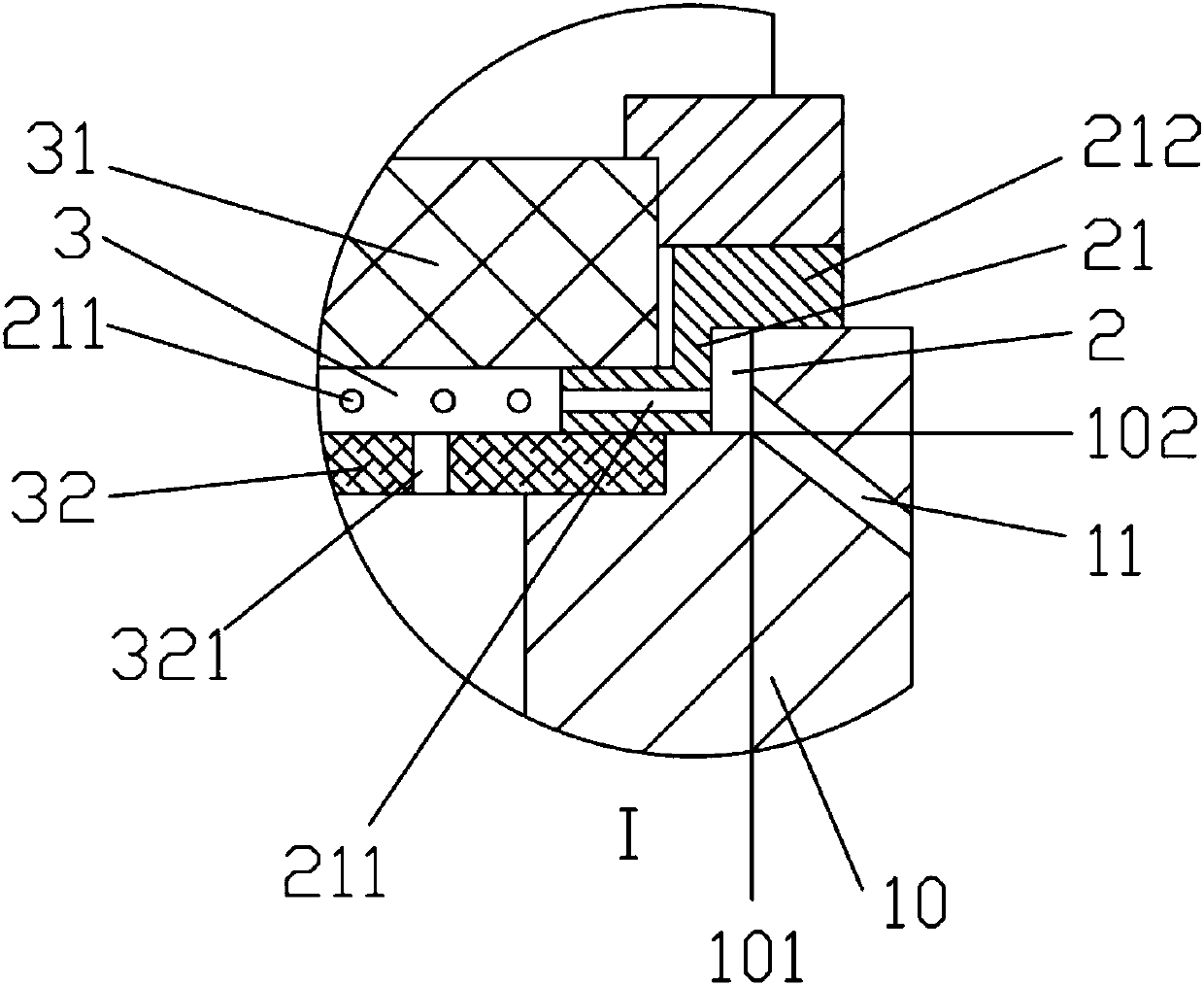
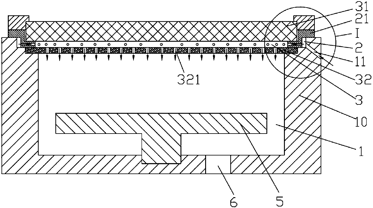
[0015] figure 1 A cross-sectional view of a heating chamber provided for an embodiment of the present invention. figure 2 for figure 1 Zoom-in view of the middle I region. Please also refer to figure 1 and figure 2 , the heating chamber 1 includes a susceptor 5 for carrying a wafer, and an air inlet mechanism for delivering process gas into the heating chamber 1 . Wherein, the intake mechanism includes a primary uniform flow chamber 2 and a secondary uniform flow chamber 3, wherein the secondary uniform flow chamber 3 is arranged above the base 5, and is evenly distributed on the bottom wall 32 of the secondary uniform flow chamber 3. A plurality of gas outlets 321 are distributed for d...


PUM


Abstract

The invention provides a heating chamber and a semiconductor processing device. The heating chamber comprises a base for carrying a wafer and an air intake mechanism. The air intake mechanism includesa first-level flow distribution chamber and a second-level flow distribution chamber, wherein the second-level flow distribution chamber is arranged above the base, a plurality of gas outlets are evenly distributed on the bottom wall of the second-level flow distribution chamber and are used for transporting process gas toward the base, the first-level flow distribution chamber is arranged aroundthe second-level flow distribution chamber and is communicated with the second-level flow distribution chamber, and the first-level flow distribution chamber is used for transporting the process gastoward the second-level flow distribution chamber. The invention provides the heating chamber, the uniformity of the process gas acting on the surface of the wafer can be improved, and so the productyield can be improved.

Description

technical field [0001] The invention relates to the field of semiconductor manufacturing, in particular to a heating chamber and semiconductor processing equipment. Background technique [0002] In the integrated circuit manufacturing process, there are liquid environment processes such as etching and CMP. After these processes, the surface of the wafer will have some attachments from the liquid organic matter, moisture, chemical solution, etc. in the above processes. These attachments It will have a great impact on the subsequent process and reduce the product yield. Therefore, after liquid environment processes such as etching and CMP, it is necessary to add a process to remove the attachments on the wafer surface. This process is the degassing (Degas) process, that is, the wafer needs to be heated in a vacuum Heating is carried out in the chamber, so that the attachments are separated from the wafer surface through volatilization, gasification, reaction, etc., and then t...

Claims


Application Information

Patent Timeline
IPC IPC(8): H01L21/67
CPCH01L21/67098
Inventor 邱国庆
Owner BEIJING NAURA MICROELECTRONICS EQUIP CO LTD
Why Eureka
Try Eureka