Semiconductor device and forming method thereof

A semiconductor and device technology, applied in the field of semiconductor devices and their formation, can solve problems such as the need to improve electrical performance, and achieve the effect of reducing impact and improving electrical performance

Active Publication Date: 2018-03-09
SEMICON MFG INT (SHANGHAI) CORP +1
View PDF3 Cites 4 Cited by
  • Summary
  • Abstract
  • Description
  • Claims
  • Application Information

AI Technical Summary

Problems solved by technology

[0005] However, the electrical performance of semiconductor devices formed by fin field effect transistors in the prior art still needs to be improved

Method used


Image

  • Semiconductor device and forming method thereof
  • Semiconductor device and forming method thereof
  • Semiconductor device and forming method thereof

Examples


Embodiment Construction

[0032] As mentioned in the background, the electrical performance of semiconductor devices formed in the prior art needs to be improved.

[0033] Figure 1 to Figure 3 It is a structural schematic diagram of the formation process of a semiconductor device.

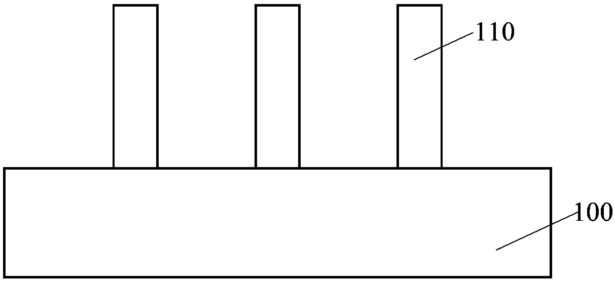
[0034] refer to figure 1 , providing a semiconductor substrate 100 having fins 110 on the semiconductor substrate 100 .

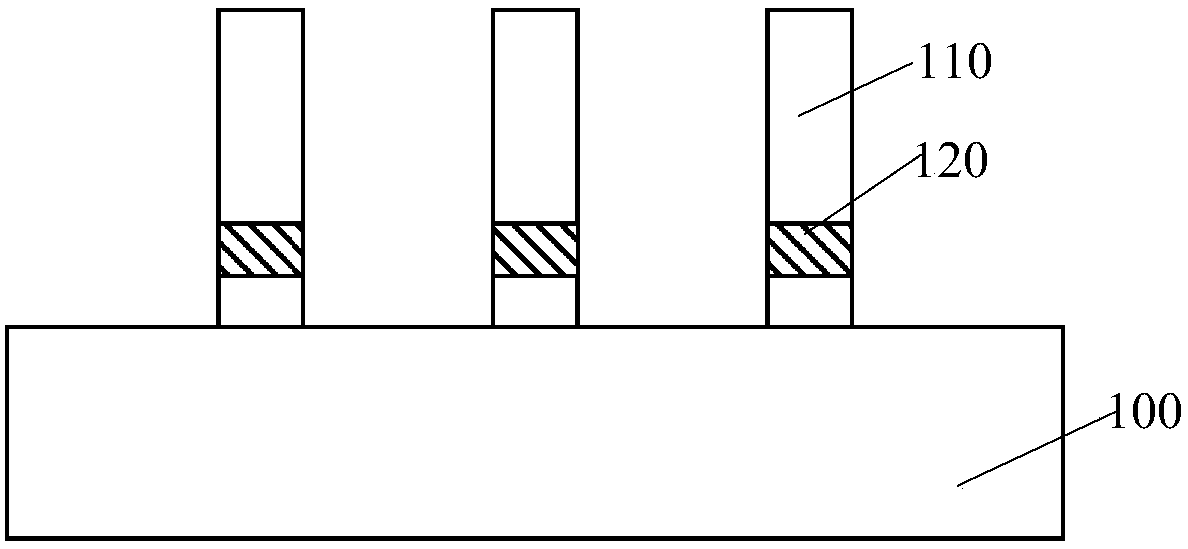
[0035] refer to figure 2 , forming an anti-penetration layer 120 in the fin portion 110 .

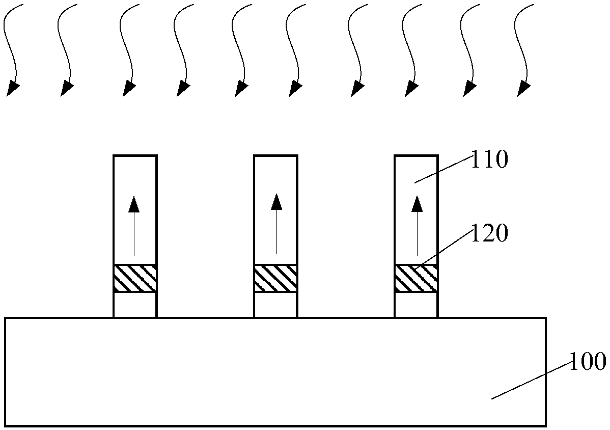
[0036] Please refer to image 3 After forming the anti-puncture layer 120, an annealing treatment is performed to activate the anti-puncture ions in the anti-puncture layer 120.

[0037] However, the electrical performance of the semiconductor device formed by the above-mentioned method is relatively poor. After research, it is found that the reasons are:

[0038] Threshold ions are doped in the channel of the semiconductor device, and the threshold ions are used to adjust the threshold voltage of the semi...


PUM


Abstract

Disclosed are a semiconductor device and a forming method thereof. The method comprises the steps of: providing a semiconductor substrate with a fin portion; forming a barrier layer with barrier ionsin the fin portion; after the barrier layer is formed, forming a punch-through preventing in the fin portion, wherein the top surface of the barrier layer is higher than or flush with the top surfaceof the punch-through preventing layer, the punch-through preventing layer has punch-through preventing ions, and the conductive type of the punch-through preventing ions is opposite to that of the barrier ions; and performing an annealing treatment after the punch-through preventing layer is formed. The method can improve the electrical properties of the semiconductor device.

Description

technical field [0001] The invention relates to the field of semiconductor manufacturing, in particular to a semiconductor device and a forming method thereof. Background technique [0002] MOS (Metal-Oxide-Semiconductor) transistors are one of the most important components in modern integrated circuits. The basic structure of the MOS transistor includes: a semiconductor substrate; a gate structure located on the surface of the semiconductor substrate, and the gate structure includes: a gate dielectric layer located on the surface of the semiconductor substrate and a gate electrode layer located on the surface of the gate dielectric layer; The source and drain doped regions in the semiconductor substrate on both sides of the pole structure. [0003] With the development of semiconductor technology, the ability of the traditional planar MOS transistor to control the channel current becomes weaker, resulting in serious leakage current. Fin Field Effect Transistor (Fin FET) i...

Claims


Application Information

Patent Timeline
Patent Type & Authority Applications(China)
IPC IPC(8): H01L29/78H01L29/06H01L21/336
CPCH01L29/0646H01L29/66803H01L29/7855
Inventor 周飞
Owner SEMICON MFG INT (SHANGHAI) CORP
Why Eureka
Try Eureka