
enhanced hfet

An enhanced, gate electrode technology, applied in semiconductor devices, electrical components, circuits, etc., can solve the problems of cascaded structure switching characteristics limitations, difficult grooving process, and large gate interface damage, etc., and achieve an ultra-wide threshold voltage region Controllable, enhanced threshold controllability, large saturation current effect

Active Publication Date: 2020-06-19
THE 13TH RES INST OF CHINA ELECTRONICS TECH GRP CORP
View PDF4 Cites 0 Cited by
  • Summary
  • Abstract
  • Description
  • Claims
  • Application Information

AI Technical Summary

Problems solved by technology

[0005] At present, the enhanced HFET based on III-nitride materials adopts an equiplanar channel layer, through grooves, F ion implantation, and cascade connection with Si devices (such as figure 1 As shown) and other ways to realize the enhanced mode, in which the groove process has great damage to the gate interface, the non-damage groove process is difficult, and the threshold value changes significantly with the groove depth; the F injection is unstable, and the switching characteristics of the cascade structure are affected by the Si Device limitations

Method used


Image

  • enhanced hfet
  • enhanced hfet
  • enhanced hfet

Examples


Embodiment 1

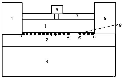
[0030] like figure 2 As shown, the embodiment of the present invention discloses an enhanced HFET, including an HFET device body. The HFET device body includes a substrate 1, the upper surface of the substrate 1 is provided with a channel layer 2, the left side of the upper surface of the channel layer 2 is provided with a source electrode 4, and the upper surface of the channel layer 2 is The drain electrode 6 is provided on the right side. A barrier layer 1 is provided on the upper surface of the channel layer between the source electrode 4 and the drain electrode 6 , and a two-dimensional electron gas (2DEG) layer is formed on the channel layer 2 below the barrier layer 1 . A two-dimensional electron gas-free region ( figure 2 Middle A to A' region), there is no two-dimensional electron gas region on the channel layer 2 between the drain electrode 6 and the source electrode 4 except for the two-dimensional electron gas region. That is to say, the two-dimensional electr...

Embodiment 2

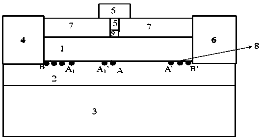
[0034] like image 3As shown, the embodiment of the present invention discloses an enhanced HFET, including an HFET device body. The HFET device body includes a substrate 1, the upper surface of the substrate 1 is provided with a channel layer 2, the left side of the upper surface of the channel layer 2 is provided with a source electrode 4, and the upper surface of the channel layer 2 is The drain electrode 6 is provided on the right side. A barrier layer 1 is provided on the upper surface of the channel layer between the source electrode 4 and the drain electrode 6 , and a two-dimensional electron gas (2DEG) layer is formed on the channel layer 2 below the barrier layer 1 . Two two-dimensional electron gas-free regions ( image 3 Middle A 1 to A 1 ' area and A to A' area), no 2DEG area formed by fluoride ion implantation.

[0035] A two-dimensional electron gas region is provided on the channel layer 2 between the drain electrode 6 and the source electrode 4 except for ...

Embodiment 3

[0037] like Figure 4 As shown, the embodiment of the present invention discloses an enhanced HFET, including an HFET device body. The HFET device body includes a substrate 1, the upper surface of the substrate 1 is provided with a channel layer 2, the left side of the upper surface of the channel layer 2 is provided with a source electrode 4, and the upper surface of the channel layer 2 is The drain electrode 6 is provided on the right side. A barrier layer 1 is provided on the upper surface of the channel layer between the source electrode 4 and the drain electrode 6 , and a two-dimensional electron gas (2DEG) layer is formed on the channel layer 2 below the barrier layer 1 . A two-dimensional electron gas-free region ( Figure 4 Middle A to A' area), no 2DEG area is formed by etching barrier layer 1.

[0038] A two-dimensional electron gas region is provided on the channel layer 2 between the drain electrode 6 and the source electrode 4 other than the two-dimensional ele...


PUM

PropertyMeasurementUnit
widthaaaaaaaaaa
widthaaaaaaaaaa
widthaaaaaaaaaa

Abstract

The invention discloses an enhanced HFET and relates to the technical field of semiconductor switching devices. The HFET includes an HFET device body. There is a two-dimensional electron gas-free region on the channel layer between the drain electrode and the source electrode of the HFET device body, and there is a two-dimensional electron gas-free zone on the channel layer other than the gate electrode. area, there is a two-dimensional electron gas area on the channel layer between the drain electrode and the source electrode outside the two-dimensional electron gas area, and the channels between the gate electrode and the source electrode and between the gate electrode and the drain electrode There are two-dimensional electron gas regions on all layers, and the channel layer directly below the gate electrode has two-dimensional electron gas partially or completely in the position of the two-dimensional electron gas layer. The HFET has the advantages of large saturation current, strong controllability of threshold voltage, fast response speed and low energy consumption.

Description

technical field [0001] The invention relates to the technical field of semiconductor switching devices, in particular to an enhanced HFET. Background technique [0002] Document 1: "High-Performance Enhancement-Mode AlGaN / GaN HFETs Using Fluoride-Based Plasma Treatment. IEEE Electron Device Letters", Yong Cai, Yugang Zhou, Kevin J. Chen , and Kei May Lau., 2005, 26(7), pp.435-437 used F plasma treatment to realize the transfer of the threshold voltage of the device. The threshold voltage of the device was increased from -4V to 0.9V, and an enhanced device was realized. [0003] Document 2: "Development and Characteristic Analysis of Enhanced AlGaN / GaN Trench Gate HFET". Hao Yue, Wang Chong, Ni Jinyu, Feng Qian, Zhang Jincheng, Mao Wei. Chinese Science Series E, 39 (1), 2009, pp.119 In -123, the threshold voltage of the device is increased from -2.2V to 0.47V by using the under-gate trenching technology. [0004] Document 3: "Simulation Model Development and Verification f...

Claims


Application Information

Patent Timeline
Patent Type & Authority Patents(China)
IPC IPC(8): H01L29/778H01L29/06H01L29/423
CPCH01L29/0684H01L29/42356H01L29/778H01L29/7786H01L29/2003H01L29/207H01L29/0649H01L29/0657H01L29/42316
Inventor 王元刚冯志红吕元杰谭鑫宋旭波周幸叶房玉龙顾国栋郭红雨蔡树军
Owner THE 13TH RES INST OF CHINA ELECTRONICS TECH GRP CORP
Learn More