Apparatus for testing semiconductor devices

A technology for semiconductors and devices, applied in the field of devices for testing semiconductor devices, can solve problems such as alignment difficulties, misalignment of solder balls, deformation of support films, etc., and achieve the goals of improving alignment accuracy, stabilizing alignment, and improving test reliability Effect

Inactive Publication Date: 2018-03-13
ISC CO LTD
View PDF8 Cites 2 Cited by
  • Summary
  • Abstract
  • Description
  • Claims
  • Application Information

AI Technical Summary

Problems solved by technology

[0010] On the other hand, since the solder balls of the semiconductor device are gradually reduced in size and the interval between the solder balls is gradually reduced, the alignment between the solder balls of the semiconductor device and the connection terminals of the test socket becomes more difficult, which can lead to lead-through Misalignment between the holes and the solder balls of the semiconductor components that should be caught in the guide holes of the support film
Furthermore, correcting such misalignment beyond a certain range may be difficult and the support film may deform due to physical forces

Method used


Image

  • Apparatus for testing semiconductor devices
  • Apparatus for testing semiconductor devices
  • Apparatus for testing semiconductor devices

Examples


Embodiment Construction

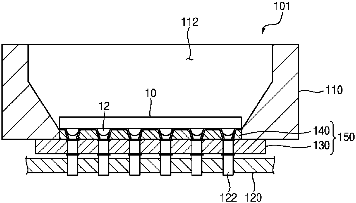
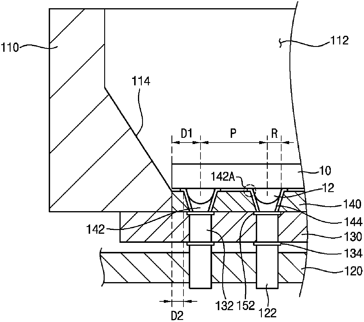
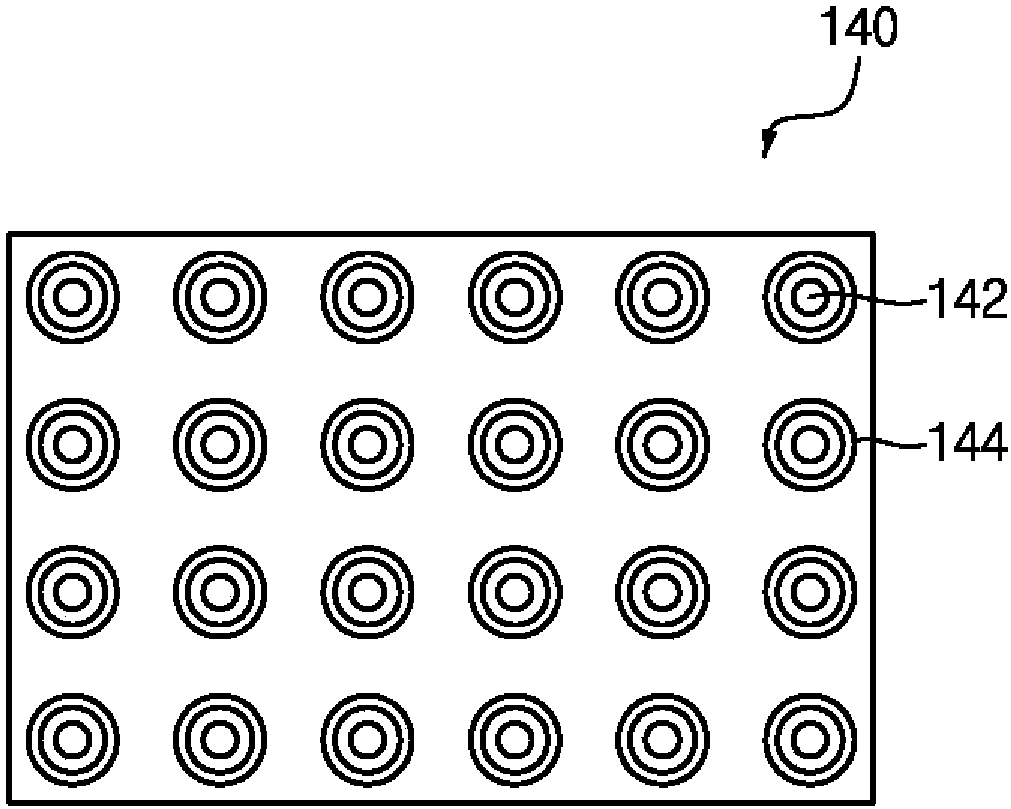
[0030] The present invention will be described more fully hereinafter with reference to the accompanying drawings, in which embodiments of the invention are shown. However, this invention may be embodied in many different forms and should not be construed as limited to only the embodiments set forth herein. Rather, these embodiments are provided so that this disclosure will be thorough and complete, and will fully convey the scope of the invention to those skilled in the art. In the drawings, the size and relative sizes of layers and regions may be exaggerated for clarity.

[0031] It will be understood that when an element or layer is referred to as being "on," "connected" or "coupled" to another element or layer, it can be directly on, directly connected to, or "coupled to" the other element or layer. may be coupled to other elements or layers, or intervening elements or layers may be present. In contrast, when an element is referred to as being "directly on," "directly co...


PUM


Abstract

A test apparatus for testing semiconductor devices include an insert including an accommodating part receiving a semiconductor device and an opening part formed on the bottom surface of the accommodating part; a test socket provided with a plurality of connection terminals electrically connecting the semiconductor device to a tester; and an interposer disposed between the insert and the test socket and electrically connecting the semiconductor device to the test socket. Especially, the interposer comprises a first circuit board disposed on the test socket, and a second circuit board coupled tothe upper surface of the first circuit board, wherein the first circuit board comprises a plurality of via contacts connected between connection terminals and contact terminals of the semiconductor device so as to connect the contact terminals to the connection terminals, and the second circuit board comprises a plurality of guide holes into which the contact terminals are inserted. Accordingly,the apparatus can protect the contact terminals from being clamped, can accurately align with a semiconductor device having a small interval, and can stably connect the contact terminals to the connection terminals.

Description

technical field [0001] Exemplary embodiments of the present invention relate to an apparatus for testing a semiconductor device. More particularly, exemplary embodiments of the present invention relate to a semiconductor device testing apparatus for testing electrical characteristics of the semiconductor device by supplying a test signal thereto. Background technique [0002] Generally, a semiconductor device can be formed on a silicon wafer used as a semiconductor substrate by repeatedly performing a series of manufacturing steps, and the semiconductor device can be manufactured into a finished product by further performing a dicing process, a bonding process, and a packaging process. [0003] A semiconductor device can be judged as good or defective by a test procedure for checking electrical characteristics of the semiconductor device. An apparatus for testing semiconductor devices can be used to perform the testing step. The apparatus for testing the semiconductor devi...

Claims


Application Information

Patent Timeline
Patent Type & Authority Applications(China)
IPC IPC(8): G01R31/26
CPCG01R31/2601G01R1/0483G01R31/2886G01R31/2889G01R31/2891
Inventor 柳正虎严基象
Owner ISC CO LTD
Why Eureka
Try Eureka