Lateral double-diffused transistor for simultaneously optimizing element semiconductor by transverse and longitudinal electric fields

A lateral double-diffusion and semiconductor technology, which is applied in the direction of semiconductor devices, semiconductor/solid-state device manufacturing, electrical components, etc., can solve the problem of limited optimization effect of lateral electric field

Inactive Publication Date: 2018-03-13
XIDIAN UNIV
View PDF2 Cites 0 Cited by
  • Summary
  • Abstract
  • Description
  • Claims
  • Application Information

AI Technical Summary

Problems solved by technology

[0006] The above two schemes are actually optimized for the vertical electric field of the device, but the optimization effect for the horizontal electric field is very limited

Method used


Image

  • Lateral double-diffused transistor for simultaneously optimizing element semiconductor by transverse and longitudinal electric fields
  • Lateral double-diffused transistor for simultaneously optimizing element semiconductor by transverse and longitudinal electric fields
  • Lateral double-diffused transistor for simultaneously optimizing element semiconductor by transverse and longitudinal electric fields

Examples


Embodiment Construction

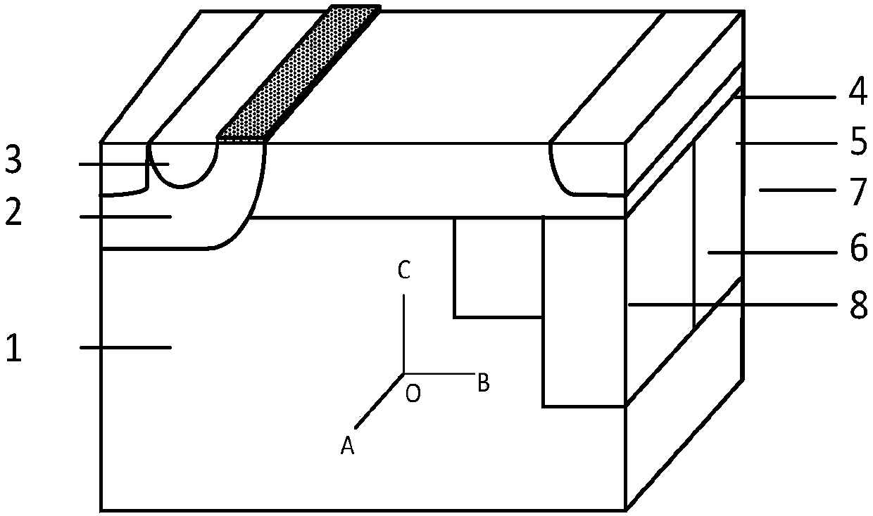
[0043] Such as figure 1 , figure 2 and image 3 Shown is a horizontal double-diffused transistor with horizontal and vertical electric fields while optimizing elemental semiconductors:

[0044] Substrate 1 of elemental semiconductor material, the doping concentration is the concentration of general elemental semiconductor single crystal material, the typical value is 1×10 13 cm -3 ~1×10 15 cm -3 ;

[0045] a base region 2 and a drift region 5 located on the surface of the elemental semiconductor substrate;

[0046] a source region 3 located on the surface of said base region;

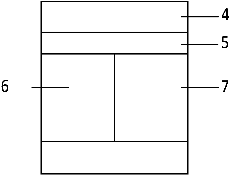
[0047] The drain region 4 located on the surface of the drift region;

[0048] Below the drift region at the drain end are vertical auxiliary depletion substrate buried layers 6 and 7;

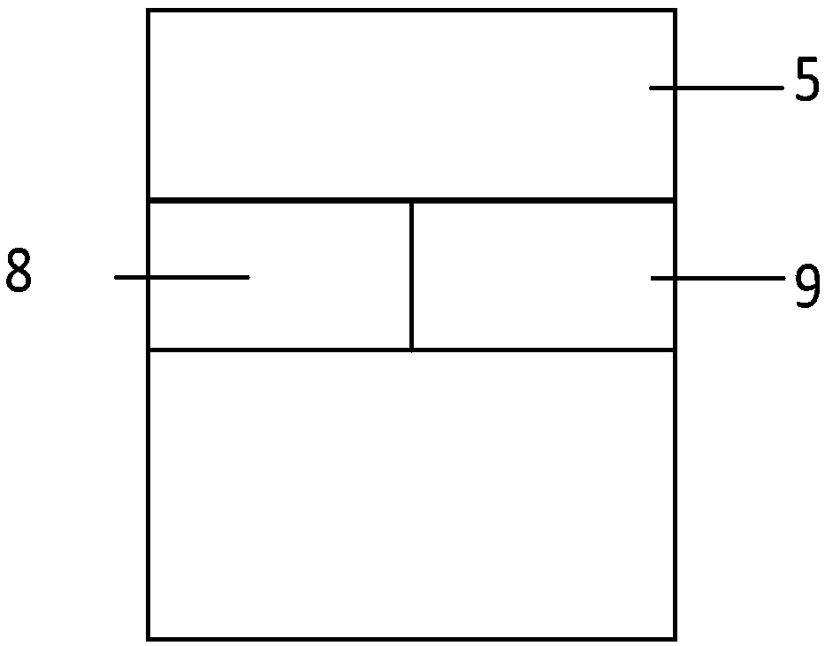
[0049] The substrate region located below the drift region and close to the vertical auxiliary depleted substrate buried layer has partial charge compensation buried substrate layers 8 and 9 .

[0050] The vert...


PUM


Abstract

The invention discloses a lateral double-diffused transistor for simultaneously optimizing an element semiconductor by transverse and longitudinal electric fields. In the structure, an auxiliary depleted substrate buried layer is arranged blow a drift region at a drain end, a substrate buried layer having partial charge compensation is arranged at a position, near to a substrate region of the auxiliary depleted substrate buried layer, below the drift region of a lateral double-diffused metal-oxide-semiconductor (LDMOS), a new electric field peak is introduced to a horizontal electric field ona surface of the device, so that the horizontal electric field on the surface of the device is more uniform in distribution, the horizontal electric field on the surface of the device is optimized very well, and meanwhile, a new electric field peak is also introduced into distribution of the longitudinal electric field in a device body so that the longitudinal electric field in the body can be further optimized. By the structure, a voltage saturation phenomenon brought by longitudinal voltage resistant limitation is broken through, most importantly, the transverse electric field on the surfaceand the longitudinal electric field in the body can be practically and simultaneously optimized, and the breakdown voltage of the device is substantially increased.

Description

technical field [0001] The invention relates to the technical field of semiconductor power devices, in particular to an optimized lateral double-diffusion transistor. Background technique [0002] Lateral Double-diffused MOSFET (LDMOS) has the advantages of easy integration, good thermal stability, good frequency stability, low power consumption, multi-subconduction, small power drive, and switching speed Advanced advantages are at the heart of smart power circuits and high-voltage devices. Due to the growing market demand for portable power management and automotive electronics, it is receiving increasing attention across the globe. Its main feature is that a relatively long lightly doped drift region is added between the base region and the drain region, and the doping type of the drift region is consistent with that of the drain region. By adding the drift region, it can share the breakdown voltage, improve the breakdown voltage of the LDMOS, make it achieve the optimiz...

Claims


Application Information

Patent Timeline
Patent Type & Authority Applications(China)
IPC IPC(8): H01L29/78H01L29/06H01L21/336
CPCH01L29/0623H01L29/66681H01L29/7823
Inventor 段宝兴董自明杨银堂
Owner XIDIAN UNIV
Why Eureka
Try Eureka