A wide-bandgap semiconductor lateral double-diffused transistor with multi-ring electric field modulation substrate

A lateral double-diffusion, semiconductor technology, used in semiconductor devices, semiconductor/solid-state device manufacturing, circuits, etc., can solve problems such as device breakdown voltage limited vertical withstand voltage capability, etc., to optimize the surface lateral electric field and body longitudinal electric field, The effect of increasing the breakdown voltage

Active Publication Date: 2021-06-18
XIDIAN UNIV
View PDF5 Cites 0 Cited by
  • Summary
  • Abstract
  • Description
  • Claims
  • Application Information

AI Technical Summary

Problems solved by technology

However, as the length of the device drift region increases, the breakdown voltage of the device is mainly limited by the vertical withstand voltage capability in the body, that is, due to the voltage saturation effect of the lateral power device, the breakdown voltage of the device gradually tends to saturation

Method used


Image

  • A wide-bandgap semiconductor lateral double-diffused transistor with multi-ring electric field modulation substrate
  • A wide-bandgap semiconductor lateral double-diffused transistor with multi-ring electric field modulation substrate

Examples


Embodiment Construction

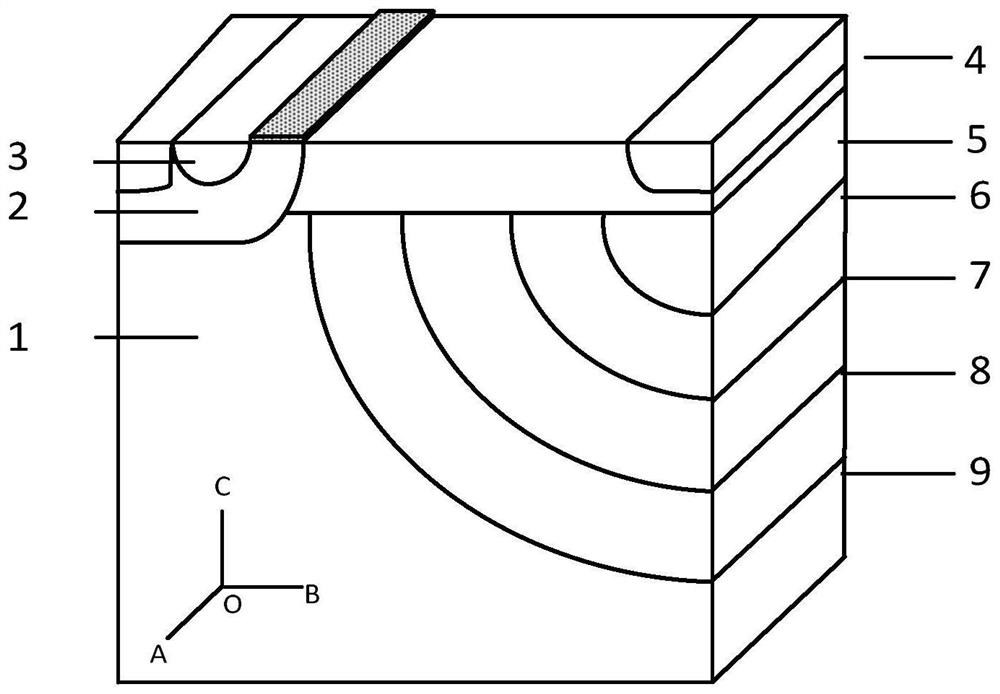
[0038] Such as figure 1 and figure 2 A wide-bandgap semiconductor lateral double-diffused transistor with a multi-ring electric-field-modulated substrate is shown:

[0039] Wide bandgap semiconductor material substrate 1, the doping concentration is the concentration of general wide bandgap semiconductor single crystal material, the typical value is 1×10 13 cm -3 ~1×10 15 cm -3 ;

[0040] The base region 2 and the drift region 5 located on the surface of the wide bandgap semiconductor substrate;

[0041] a source region 3 located on the surface of the base region;

[0042] The drain region 4 located on the surface of the drift region;

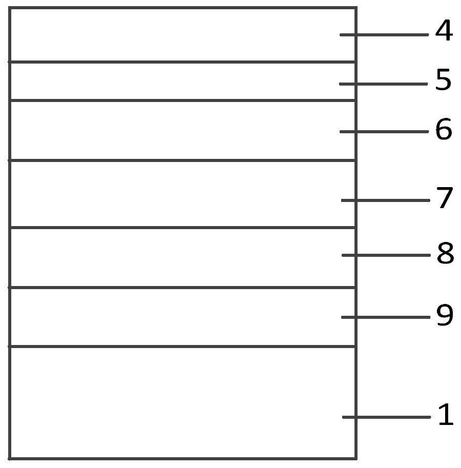
[0043] A multi-ring electric field modulation structure located under the drift region;

[0044] The rings 6, 7, 8 and 9 of the multi-ring electric field modulation structure can be N-type and P-type doped silicon materials, and the typical doping concentration reaches 1×10 14 cm -3 ~1×10 16 cm -3 ;

[0045] Each ring 6, 7, 8 and ...


PUM


Abstract

The invention discloses a wide-bandgap semiconductor lateral double-diffusion transistor with a multi-ring electric field modulation substrate. The substrate under the drift region in this structure is a charge compensation polyring structure. The multi-ring charge compensation of the substrate can expand the vertical space charge region of the lateral double-diffused metal oxide semiconductor field effect transistor. The modulation effect simultaneously modulates the surface transverse electric field and the body longitudinal electric field, so that the surface transverse electric field and the body longitudinal electric field are simultaneously optimized. This structure not only breaks through the breakdown voltage saturation problem of the lateral double-diffused transistor due to the limited vertical withstand voltage, but also achieves the simultaneous optimization of the surface lateral electric field and the internal vertical electric field, which can greatly increase the breakdown voltage of the device.

Description

technical field [0001] The invention relates to the technical field of semiconductor power devices, in particular to a lateral double-diffused metal oxide semiconductor field effect transistor. Background technique [0002] Lateral Double-diffused MOSFET (LDMOS) has the advantages of easy integration, good thermal stability, good frequency stability, low power consumption, multi-subconduction, small power drive, and switching speed Advanced advantages are at the heart of smart power circuits and high-voltage devices. Due to the growing market demand for portable power management and automotive electronics, it is receiving increasing attention across the globe. [0003] However, due to the limitations of the first two generations of semiconductor materials represented by Si and GaAs, the third generation of wide-bandgap semiconductor materials has developed rapidly because of its excellent performance. Wide bandgap semiconductor materials have the characteristics of large b...

Claims


Application Information

Patent Timeline
Patent Type & Authority Patents(China)
IPC IPC(8): H01L29/78H01L21/336H01L29/06
CPCH01L29/0603H01L29/0611H01L29/0623H01L29/0684H01L29/66477H01L29/7816
Inventor 段宝兴杨银堂董自明
Owner XIDIAN UNIV
Why Eureka
Try Eureka